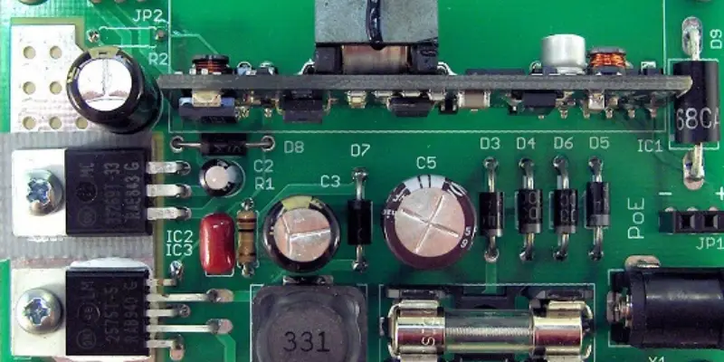
Power supply PCB plays a crucial role in the reliable and efficient operation of electronic systems. Whether you’re designing a power supply for a simple circuit or a complex application, having a well-designed power supply PCB is essential. In this comprehensive guide, we will explore the key considerations and steps involved in designing a power supply circuit board that meets the required specifications and ensures optimal performance. So let’s dive in and learn how to design a power supply PCB like a pro!
What Is Power Supply PCB?
A power supply PCB is a specialized circuit board designed to regulate and distribute electrical power to various components or subsystems within an electronic device. Its primary function is to convert the incoming electrical power from an external source, such as an AC outlet or battery, into the appropriate voltage and current levels required by the electronic device. Power supply PCBs are integral parts of almost all electronic devices, ranging from smartphones, laptops, and computers to household appliances, industrial machinery, and automotive systems. They ensure that the electronic components within these devices receive stable and reliable power, essential for their proper functioning
Power Supply PCB Design Considerations
Designing power supplies requires careful attention to PCB layout and the establishment of an efficient power distribution network. It is crucial for the designer to recognize the significance of power supply operation and its impact on overall success. To achieve this, it is crucial to meticulously carry out the PCB layout while considering the careful segregation of power supplies and circuits between noisy digital circuits and essential analog circuits. Below we list key considerations during the design process:
Choosing the Right Regulator
When selecting a regulator for your power supply, you have two main choices: linear regulators and switched-mode regulators. Linear regulators offer low noise output but have higher heat dissipation, requiring cooling systems. They also require an input voltage higher than the desired output voltage due to a voltage dropout. While linear regulators are simple, affordable, and provide noiseless outputs, they suffer from significant power loss and lower efficiency. If you opt for a linear regulator in your PCB design, choose one with a low voltage dropout and perform thermal analysis before fabrication.
On the other hand, switched-mode regulators convert voltage by storing and releasing energy in inductors. They use fast switching MOSFETs and offer highly efficient regulation. The output voltage can be altered by modifying the duty cycle of the Pulse Width Modulation (PWM). Switching regulators are more expensive and require additional passive components, but they have lower heat dissipation.
Selecting the Right Components
Choosing the right components is vital for the successful design of a power supply PCB. Take into account the voltage and current needs of your application, and choose components capable of handling the designated power levels. Pay attention to factors like component types, packages, and footprints, ensuring compatibility with your design and manufacturing constraints. Opting for reliable and reputable component suppliers will ensure the quality and longevity of your power supply design.
Thermal Management
The effectiveness of a power supply is directly influenced by its heat dissipation capabilities. When current flows through electronic components, they generate heat, the amount of which depends on their power level, characteristics, and impedance. Lower temperatures promote better performance and longevity of electronic circuits. Therefore, it is essential for designers to incorporate proper cooling methods to ensure devices operate within the desired ambient temperature range.
In the case of using a linear regulator, it is advisable to employ a heat sink or other cooling mechanisms, provided that the system allows for it. Incorporating fans can facilitate forced cooling, especially when dealing with high heat dissipation from a particular device.
Heat dissipation across the PCB may not be uniform. Components with higher power ratings tend to generate more heat, resulting in hotspots around them. To address this issue, thermal vias can be strategically placed near these components to efficiently transfer heat away from the affected areas. By combining effective heat-dissipating techniques and appropriate cooling methods, designers can achieve a highly efficient power supply design that promotes optimal performance and reliability.
Trace Routing
When it comes to trace routing, there are different approaches, such as routing during placement or after placement is complete. Regardless of the method you select, it is crucial to guarantee that your routing aligns with the component placement by employing short and straight traces. Make sure to use traces with sufficient width to handle the current requirements and opt for 45-degree or rounded corners instead of right angles to minimize signal integrity issues.
It is advisable to refrain from utilizing vias for power traces to prevent the introduction of inductance. Additionally, it’s crucial to avoid routing other signal traces under the power components to prevent interference and maintain signal integrity.
Grounding
To ensure optimal grounding for the power supply, it is recommended to create a separate ground plane for the power components. Utilizing a solid ground plane instead of routing with traces offers several advantages. Firstly, it provides an efficient grounding solution for the power supply. Additionally, it effectively isolates the noise generated by the current return paths onto a dedicated plane, keeping them separate from sensitive signal return paths on the common ground plane. In the PCB layout, the two ground planes will ultimately establish a connection at a specific juncture, commonly designated as the ground via. This ground via is typically positioned within the thermal pad beneath the power supply IC. This connection serves the purpose of joining the two planes together, while also providing a pathway for heat dissipation from the power supply. It holds particular significance in linear power supply designs. Furthermore, when designing linear power supplies, it is advisable to create a void in the ground plane specifically for high-gain devices. By doing so, potential noise interference is minimized, and the performance of these sensitive components can be enhanced.
Power Traces and Copper Pour
Calculating trace widths and ensuring proper copper thickness are essential for carrying the required current without excessive voltage drops or overheating. Utilize trace width calculators and PCB design software to determine appropriate trace widths based on the current-carrying capacity. Additionally, consider implementing copper pour techniques to enhance heat dissipation and improve the overall thermal performance of your power supply PCB. Ground planes can be utilized effectively to minimize noise and improve signal integrity.
Power integrity
Power integrity refers to the quality of power delivered to the circuit, measuring how effectively power is transferred from the source to the load within a system. It ensures that all circuits and devices receive the necessary power to achieve the desired performance.
One key aspect of maintaining power integrity is minimizing noise in the power supply. A power supply with low noise levels contributes to higher power integrity. Designing for power integrity involves effectively managing power supply noise. There are various simulation tools accessible for estimating the power quality within a circuit. These tools can help predict voltage drops, recommend the placement of decoupling capacitors, and identify areas of high current flow, known as hotspots, within the circuits.
Conclusion
Creating a power supply PCB necessitates meticulous attention to numerous factors. By adhering to this all-inclusive manual, you can design power supply PCBs that fulfill the necessary specifications and provide dependable and efficient performance.
As a renowned PCB manufacturer, MOKO Technology boasts an extensive range of state-of-the-art equipment and expertise in processing power supply PCBs. We are capable of customizing power supply PCB solutions according to your specific needs, from design to manufacturing and testing. Click here for a free consultation.