With the ongoing miniaturization and complexity of electronic devices, maximizing PCB space and trace routing has become critical. Fitting ever-growing component counts into tight PCB spaces is an ongoing challenge. This need for dense, efficient PCB layouts drives the widespread adoption of double sided PCB. With traces on both top and bottom, double-sided PCBs maximize usable space. This guide provides a comprehensive overview of double sided printed circuit boards, aiming to help you better understand this crucial PCB technology.
What Is a Double Sided PCB?
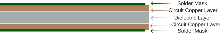
Double sided PCB refers to printed circuit boards that have conductive copper traces on both the top and bottom sides. This allows for circuits and routing to be designed on each side of the board, with conductive paths linking between the two layers. The key benefit of double sided PCBs is the ability to achieve tighter trace routing versus single sided boards. With circuits and traces on both sides, components can be more densely packed and complex interconnections facilitated. This makes double sided PCBs ideal for many modern compact consumer electronics and complex circuit designs. The dual sided layout is enabled by a dielectric substrate layer separating the bottom and top copper layers, which electrically isolates them while allowing targeted connections between layers. The picture below can help you better understand the structure of double-sided PCB:
How to Manufacture Double Sided PCB?
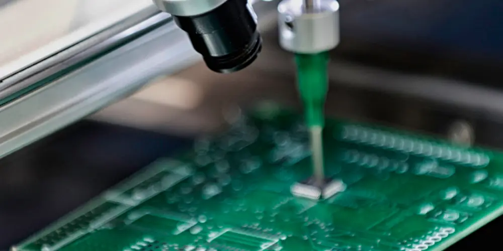
The fabrication of double sided printed circuit boards involves a multi-step process that enables circuit traces and components on both the top and bottom of the board. Manufacturing starts with the raw PCB laminate, made up of a dielectric substrate such as FR-4 sandwiched between two thin copper layers that will form the conductive traces. The process involves:
- Imaging
A photoresist is applied on the copper layers and UV light is used to transfer the trace patterns onto the PCB. The unexposed photoresist is then washed away, exposing the copper for etching.
- Etching
Chemical etchants are used to remove the unwanted copper, leaving only the desired copper traces on each layer.
- Hole drilling
Holes are drilled through the board to facilitate component mounting and connections between layers.
- Plating
The walls of the drilled holes are plated with copper to enable conductivity between layers.
- Solder mask application
A solder mask is applied over the entire PCB surface except the exposed pads and traces. This prevents solder bridges.
- Silkscreen printing
Identifying markings, symbols and labels are printed onto the board.
- Final finishing
The boards are cut, beveled, tested and quality checked before being shipped out.
Want to know more knowledge about PCB manufacturing? Check out our other blog: A Detailed Guide to the PCB Manufacturing Process
Advantages of Double Sided PCB Board
- Increased Component Density
With a double sided PCB, components can be placed on both the top and bottom sides of the board. This significantly increases the component density compared to a single sided PCB, allowing more complex circuits to be designed within the same limited space. The dual-sided nature doubles the usable area for placing components.
- Better Routing Options
Double sided circuit board has more routing options available. Traces can be routed efficiently on either side of the board, enabling optimized use of the available space. This leads to shorter trace lengths and more effective layouts. The ability to route across both layers provides more flexibility.
- Improved Signal Integrity
Double sided PCB construction better controls signal traces compared to single sided boards. Designers can carefully plan the layout of traces on the different layers to reduce signal interference and crosstalk. The isolation between layers provides more control.
- Compact Design
Double-sided PCBs enable more compact electronic device designs by utilizing both sides of the board. This allows the overall PCB size to be reduced, ideal for space-constrained applications. Single sided boards limit layout options, but double-sided provides more usable area.
- Enhanced Grounding and Power Distribution
With double-sided PCBs, dedicated ground and power planes can be designed on opposite sides. Separating the planes helps provide stable, efficient power and grounding, reducing noise. This is crucial for smooth circuit operation.
- Support for Complex Circuits
The large number of connections in complex circuits like those with microcontrollers often require double-sided PCBs. The dual-layer routing provides the needed options to handle intricate multi-connection designs.
Design Considerations of Utilizing Double Sided PCB
Component Placement – Optimal component placement is crucial for efficient routing. Place related components on the same side when possible, with consideration for board thickness and heat dissipation.
Routing Channels – Carefully plan routing channels to isolate critical signals and avoid crosstalk. Use wider spaces between traces or ground planes as barriers.
Layer Stacking – Mindfully stack layers, keeping similar signals together. Route critical traces on the top layer first with ground planes below.
Via Usage – Use vias judiciously between layers for connections. Minimize via count for cost savings but allow enough for required connections.
Further reading: What is PCB Via?
Trace Length Matching – Match the lengths of traces in differential pairs and high speed traces to control skew and timing. Consider how traces route on both layers.
Grounding – Properly ground components with vias tied to the ground plane. Separate analog and digital ground planes.
Board Thickness – Thicker boards handle more layers and complex routing but increase weight and cost. Optimize thickness for needs.
Thermal Management- Ensure there is a proper thermal relief, and consider adding thermal vias to dissipate heat away from sensitive components. Adequate spacing between heat-generating components can also assist in heat dissipation.
Applications of Double Sided Circuit Boards
There are numerous applications of double-sided PCBs. We can find them in Computers, TVs, Digital Cameras, Radios, Cell Phones, and other electronic gadgets. They have many industrial applications as well and we will look at some of them.
- Medical devices
Modern medical equipment consumes less power and is denser than it was in the past. Therefore, we need such PCBs which have small size and large surface area because this will help us in incorporating more electronic components. Double sided PCB board is ideal for this as it has two layers and we can incorporate electronic components on both of them. This way we get the desired properties of both the lightweight and little sizes. Therefore, we use it in a number of medical devices such as the CAT scanner and X-ray scanner.
- Mechanical Systems
We often use PCBs for control processes in heavy-powered mechanical systems. Single layer PCB has a small density and doesn’t suit the performance requirements in such conditions. Therefore, we need denser PCBs and double-sided PCB is a viable option. They can incorporate components like high-current battery chargers, modern load analyzers, and engine controllers.
- Lighting
We widely use LEDs because of their improved productivity and low power consumption. We often use LEDs where we need them to frequently turn on and off. This means that there are high current and voltage cycles. So, we can’t use ordinary PCBs because they can’t withstand the generated heat. Double sided PCB is suited for this because they have two insulating layers. These PCBs will act as warmth sinks and can withstand elevated temperatures of heat exchange.
- Automotive and aerospace
Both of these industries frequently rely on adaptable PCBs. We use double sided printed circuit board in both the automotive and aviation ventures because they can withstand high-vibrations which are normal to their surface. To simply put, they can withstand forces which are exerted on them from both the top and bottom layer. On top of this, double sided PCB is very lightweight. So, they are ideal for using them in transportation applications.
MOKO Technology is a well-known entity when it comes to the manufacturing of printed circuit boards. We have years of expertise and we specialize in the manufacturing of double-sided PCBs. We have a well-trained staff, a dedicated R&D team, and a state-of-the-art setup. This allows us to boast mass production capability. We provide premium quality PCBs that will meet your requirements. We can also manufacture custom made PCBs as per your needs. Feel free to reach out to us if you have any questions or if you want a quote. We are hoping to hear from you soon.