Is it advisable to avoid vias in a PCB layout as much as possible?

When we design PCB, for some layout can, via is dispensable. Particularly if the PCB has more than 2 layers, should I make it?

Vias, usually small holes, are drilled quickly. They connect all the layers and are plated in a single mass operation, so the incremental cost is very low. They are usually quite reliable and have a small resistance for slow circuits.

The reasons for avoiding vias are possible

  • Impedance discontinuities
  • Several milliohms of resistance for large current
  • another good solution, such as using vertical trace on one layer and horizontal on another,
  •  Not applicable to critical high-speed controlled impedance paths because they run first.
  • Less reliable than a straight trace

Certainly, if you want to use a multilayer board – 4 layers or more, they are the ticket to using all the layers effectively. You can’t do without them.

#PCB Design
Picture of Oliver Smith

Oliver Smith

Oliver is an experienced electronics engineer skilled in PCB design, analog circuits, embedded systems, and prototyping. His deep knowledge spans schematic capture, firmware coding, simulation, layout, testing, and troubleshooting. Oliver excels at taking projects from concept to mass production using his electrical design talents and mechanical aptitude.

What Others Are Asking

How common is it to receive PCBs with failed or weak vias?

We had a number of flexi-rigid PCBs fabricated and assembled by a company in the UK. When the boards arrived and we tested them, we discovered a couple of failed vias, which we fixed with jumper wires. How common is it to receive PCBs with failed or weak vias?

Read Detailed Advice From Blog Articles

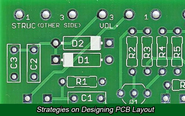
Strategies on Designing PCB Layout
Ryan Chan

Strategies on Designing PCB Layout

Why PCB Layout is Needed We use Printed Circuit Boards (PCB) for connecting electronic components by using conductive tracks. This allows for prototyping electric circuits

Scroll to Top