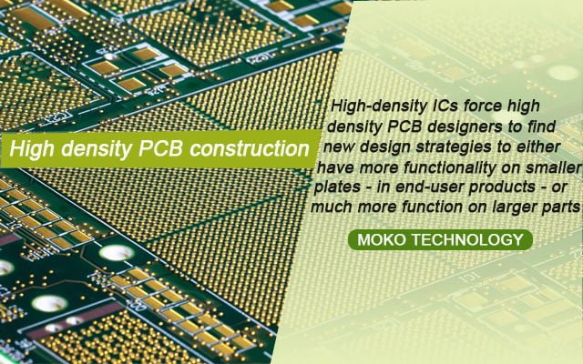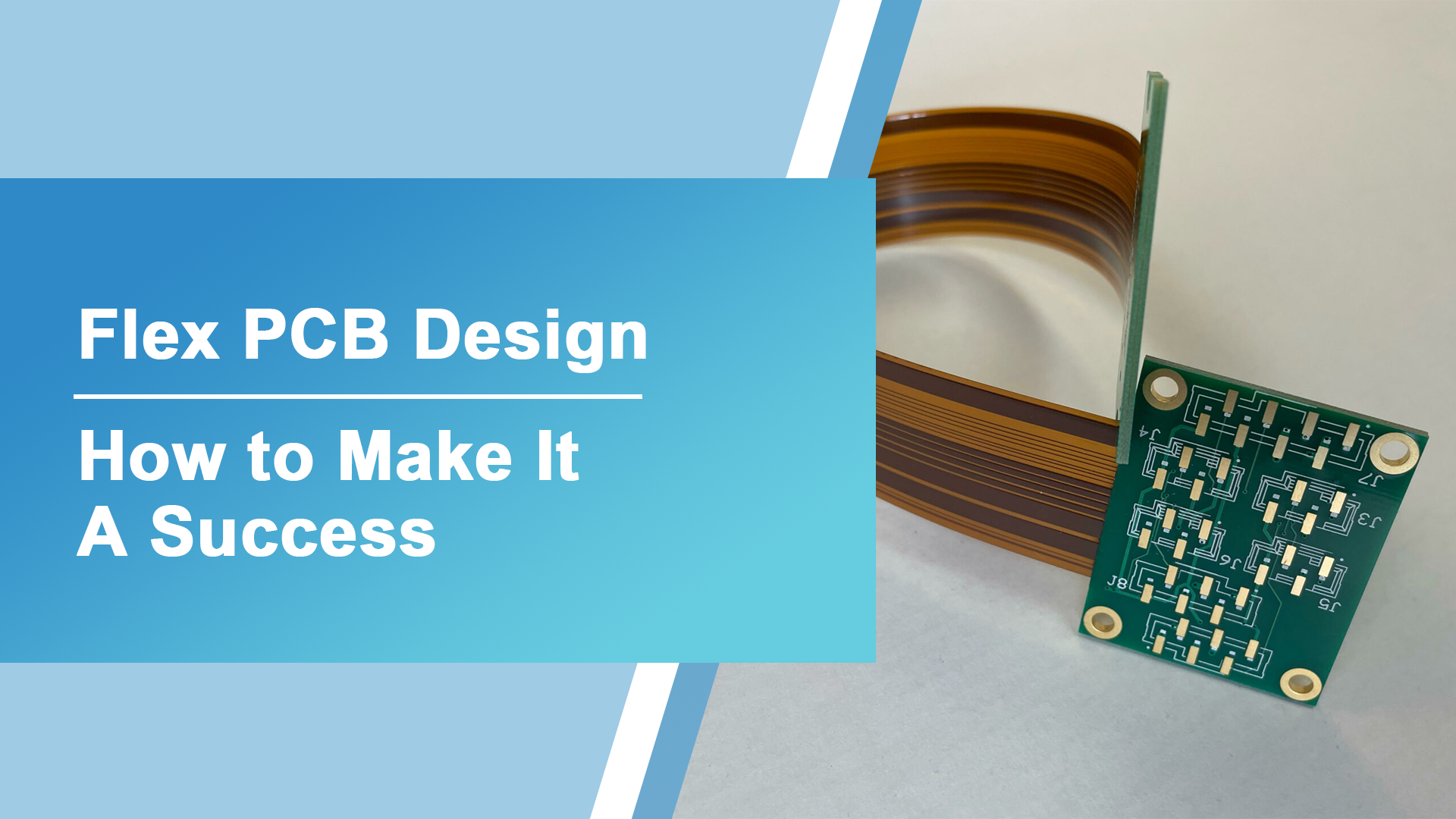
Flex PCBs, or Flexible Printed Circuit Boards, have gained significant popularity in recent years due to their unique properties and advantages in various applications. These thin, lightweight, and flexible circuit boards offer a host of benefits over traditional rigid PCBs, such as improved space utilization, reduced weight and volume, enhanced durability, and increased design flexibility. In this blog, we will explore the key considerations, potential problems to avoid, and tips for making your flex PCB design a success.
What Is Flex PCB?
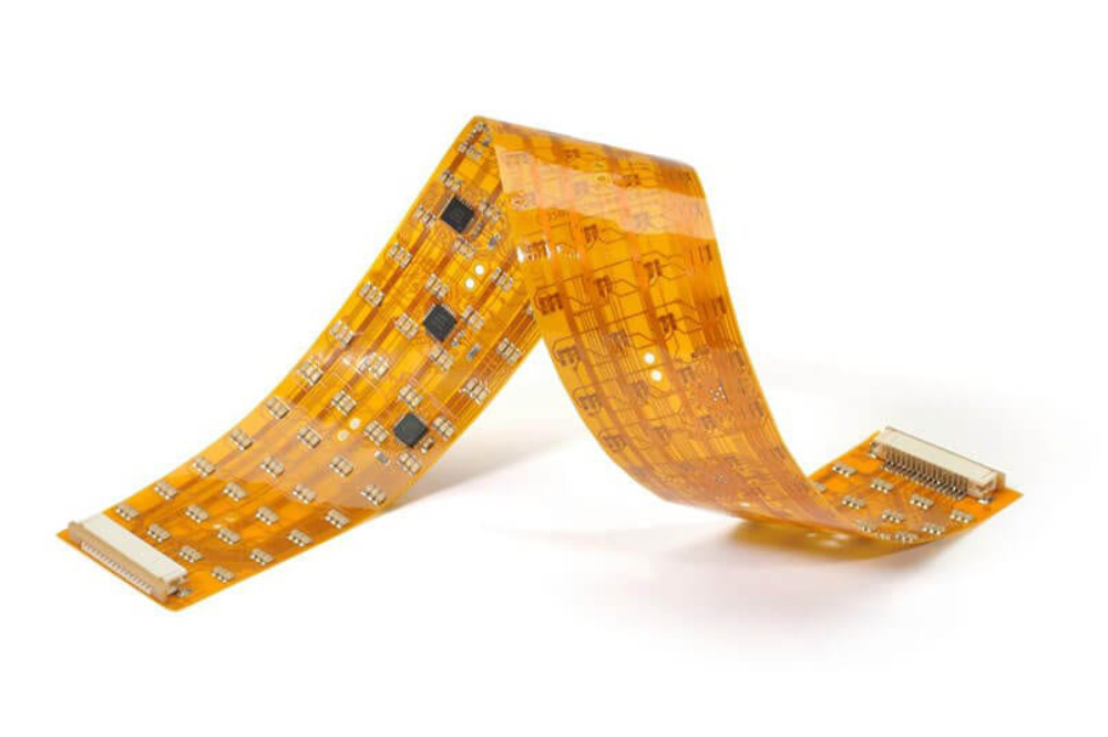
Flex PCB, as the name suggests, is a type of printed circuit board that is designed to be flexible and bendable. It consists of a thin layer of conductive traces and insulating layers, which are made of polyimide or polyester films that are capable of bending and flexing without damaging the circuitry. The conductive traces are typically made of copper, and they can be either rigid or flexible, depending on the design requirements.
Flex PCBs come in various types, including single-sided flex PCBs, double-sided flex PCBs, and multilayer flex PCBs. Single-sided flex PCBs have conductive traces on one side, while double-sided flex PCBs have conductive traces on both sides. Multilayer flex PCBs, on the other hand, have multiple layers of conductive traces and insulating layers, making them more complex but also more versatile in terms of design options.
Flexible PCB Design Considerations
Designing a flex PCB requires careful consideration of several key factors to ensure a successful outcome. Some of the critical design considerations for flex PCBs include:
Bend Radius: Flex PCBs can bend to a certain extent without damaging the circuitry. The minimum bend radius, which is the tightest radius that the flex PCB can bend without risking damage to the conductive traces, should be carefully calculated and maintained during the design process to prevent cracking or delamination of the circuitry.
Flex-to-Install Ratio: The flex-to-install ratio is the ratio of the length of the flex PCB to the length of the installation path or the distance between the two fixed points where the flex PCB is installed. This ratio determines the amount of flexing or bending that the flex PCB will undergo during operation. It is important to keep this ratio within acceptable limits to prevent damage to the circuitry.
Selecting the Right Materials: When it comes to flex PCBs, meticulous material selection is paramount to guarantee optimal performance and unwavering reliability. Polyimide and polyester films are commonly used for flex PCBs due to their flexibility, durability, and excellent electrical properties. The thickness of the materials should be carefully chosen based on the specific application requirements, taking into consideration factors such as the bend radius, flex-to-install ratio, and electrical performance.
Trace Layout: The layout of the conductive traces on the flex PCB should be carefully planned to accommodate the bending and flexing of the board. The traces should be routed in a way that minimizes stress on the circuitry during flexing and avoids sharp corners or acute angles that could lead to cracking or delamination. It is important to follow design guidelines provided by the flex PCB manufacturer to ensure proper trace layout for reliable performance.
Component Placement: The placement of components on the flex PCB should also be carefully considered. Components should be positioned in a way that minimizes stress on the flex PCB during bending or flexing. Larger or heavier components should be placed closer to the rigid parts of the board to prevent excessive stress on the flexible areas.
Connector Selection: Connectors used in flex PCB designs play a crucial role in ensuring reliable connections between the flex PCB and other components or devices. The selection of connectors should be based on their compatibility with the flex PCB material, their ability to withstand flexing and bending, and their reliability in high-stress environments.
Problems to Avoid in Flex Board Design

While flex PCBs offer many advantages, there are also potential problems that can arise if not addressed properly during the design process. Some of the common problems to avoid in flex PCB design include:
Solder joints too close to the bending point
If solder joints are positioned too close to the bend points on a Flex board, it may result in cracking or delamination of solder pads during a single bending process. To prevent this, it is best to position solder joints at a safe distance from the bend points. If space constraints make it impossible, using a jig or clamp to provide support during bending is a recommended solution to mitigate the risk of solder joint issues on the Flex board.
Poor ink transfer in flexographic printing
Uneven print density, visual inconsistencies resembling an orange peel, and poor ink transfer in flexographic printing can be caused by the condition of the flexographic plate or anilox. To mitigate these concerns, it is imperative to meticulously choose an appropriate anilox with the right cell count and volume, and diligently clean the ink-transferring elements of the anilox on a regular basis.
Uneven print density in Flex board designs
If you are experiencing uneven print density in Flex board designs, it is recommended to check the layout of the design and the printing process. It is observed that dots may appear on the print pixels, which are part of the third and fourth-pixel groups, during the third and fourth passes of the printing process. This can potentially lead to open circuits in the board design, causing connectivity issues. Regularly cleaning the bottom of the stencil can help prevent the tombstone effect and ensure consistent print density.
7 Tips for Flex PCB Design
To ensure a successful flex PCB design, here are some tips that can help you make your design even better:
- Optimize Trace Routing
Carefully route traces on the flex PCB to minimize stress on the traces during bending or flexing. Use gentle curves and avoid sharp turns. Avoid placing vias or components in areas that will be subject to excessive flexing, as they can be more prone to failure.
- Choose Appropriate Materials
Select the right materials for your flex PCB design. Consider factors such as flexibility, temperature tolerance, and environmental conditions. Choose materials that can withstand the intended operating conditions and flexing requirements of your application.
- Understand Flex PCB Design Constraints
Flex PCBs have unique design constraints due to their flexibility and bending capabilities. Familiarize yourself with these constraints, such as minimum bend radius, the maximum number of flex cycles, and available flex stackup options, and design your flex PCB accordingly.
- Plan for Flexibility
Determine the areas on the flex PCB that will require bending or flexing, and design them accordingly. Use curved or rounded shapes for these areas, and avoid sharp corners or acute angles which can result in stress concentration and potential failure.
- Follow Industry Standards
Follow industry standards and guidelines for flex PCB design, such as IPC-2223 for flex and rigid-flex PCBs. These standards provide important recommendations and best practices for designing reliable and high-quality flex PCBs.
- Perform Thorough Testing
Conduct thorough testing and validation of your flex PCB design to ensure its reliability and performance. Perform flex testing to simulate real-world conditions and verify the durability and functionality of your design.
- Use Proper Stiffeners
Stiffeners, which are additional layers added to the flex PCB to provide reinforcement, can help prevent bending or twisting of the flexible areas. Use proper stiffeners, such as polyimide or FR-4, in areas that require additional support, and ensure they are properly bonded to the flex PCB.
Final Thoughts
If you’re new to flex PCB design, it can be a complex task with many factors to consider. To ensure your design meets the required specifications and performs reliably in your application, it’s advisable to seek the help of an experienced engineer or design consultant who specializes in flex PCB design. They can provide valuable insights and guidance.
At MOKO Technology, we offer top-notch PCB design services. With nearly 20 years of experience in the field, our team has the expertise and capacity to deliver the best flex board design and fabrication services. Contact us today to learn more about our one-stop PCB services or to consult with our experts for your next flex PCB project.