Multilayer PCBs(Printed Circuit Boards) have become a critical component in modern electronics due to their ability to offer higher density, improved signal integrity, and efficient thermal management. As electronic devices continue to increase in complexity, the design of multilayer PCBs plays a crucial role in ensuring optimal performance and reliability. In this comprehensive guide, we will delve into the basics of multilayer PCB design, covering important factors to consider, best practices, and troubleshooting tips for creating high-quality multilayer PCB designs. Whether you are a seasoned designer or new to PCB design, this guide will provide valuable insights and practical guidance for making your multilayer PCB design even better.
Basics of Multilayer PCB Design
To understand multilayer PCB design, let’s first define what a PCB is. A PCB is a thin board made of insulating material, such as fiberglass, with conductive pathways, known as traces, printed on it. These traces connect various components, such as resistors, capacitors, and integrated circuits, to create a functioning electronic circuit.
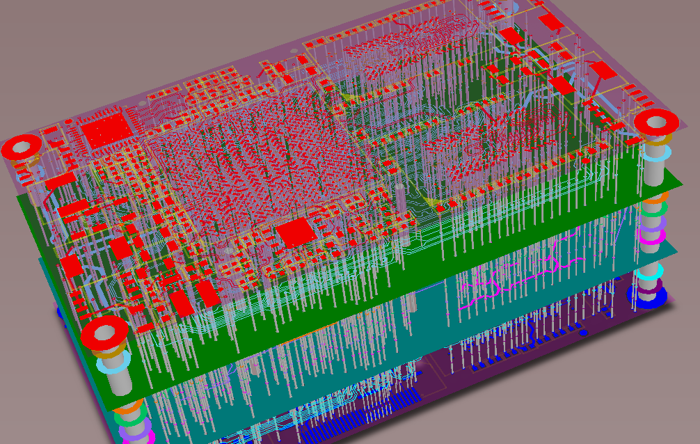
In a multilayer PCB, multiple layers of insulating material are stacked together, with traces printed on each layer. These layers are interconnected using vias, which are small holes drilled through the layers and plated with conductive material. The number of layers in a multilayer PCB can vary depending on the complexity of the circuit and the design requirements.
Compared to single-layer and double-layer PCBs, multilayer PCBs offer several advantages. They allow for higher circuit density, as components can be placed on both sides of the board and interconnected through multiple layers. They also provide better signal integrity, as traces can be routed on different layers to minimize interference. In addition, multilayer PCBs can efficiently manage heat generated by components, thanks to the presence of power and ground planes.
Factors to Consider in Multilayer PCB Design
Designing a multilayer PCB involves several critical factors that need to be considered to ensure optimal performance and reliability:
Signal Integrity
Signal integrity refers to the quality of signals transmitted through traces on a PCB. Factors such as impedance control, transmission line effects, and EMI/EMC considerations can significantly impact signal integrity. And we should pay attention to routing high-speed signals, avoiding reflections, and minimizing noise to ensure reliable signal transmission.
Power Integrity
Power integrity is crucial for the stable and reliable operation of electronic circuits. Designing a proper power distribution network (PDN), placing decoupling capacitors strategically, and optimizing power plane design are important considerations in multilayer PCB design to minimize power-related issues, such as voltage drops and ground bounce.
Thermal Considerations
The dissipation of heat plays a pivotal role in the performance and reliability of electronic circuits. It is imperative to carefully consider the placement of components, incorporate thermal vias, and utilize copper pours as effective measures to regulate and prevent overheating, particularly in demanding applications involving high power or elevated temperatures.
Layout Considerations
Efficient performance of a multilayer printed circuit board heavily relies on the strategic arrangement of its components. It is vital to consider factors such as proper component placement, routing techniques, and adherence to clearance and spacing requirements in order to ensure optimal signal transmission, minimal noise interference, and streamlined assembly and testing processes.
Design for Manufacturability (DFM)
Ensuring that a multilayer PCB is designed with manufacturability and assembly-friendliness in mind can avoid costly rework and delays in the production process. Factors such as panelization, solder mask design, and copper balance are critical DFM considerations that must be carefully taken into account. Proper panelization techniques, well-thought-out solder mask designs, and balanced copper distribution are important aspects to consider in order to optimize the manufacturing and assembly processes, reduce potential issues, and ensure smooth production flow without costly setbacks.
Best Practices in Multilayer Circuit Board Design
Following industry best practices is essential for designing high-quality multilayer PCBs, some of the best practices include:
- Use of Appropriate Design Tools
Utilize advanced design tools specifically designed for multilayer PCB design, such as Altium Designer, Cadence Allegro, or Mentor Graphics PADS. These tools offer advanced features, such as impedance control, layer stack-up management, and signal integrity analysis, that can greatly aid in the design process and ensure optimal performance.
- Careful Layer Stack-up Planning
Strategize the layer stack-up meticulously in line with the design prerequisites, encompassing signal integrity, power integrity, and thermal management. For optimal performance, it is necessary to consider factors such as the number of layers, material selection, and individual layer thickness.
- Impedance Control
Impedance control is crucial for high-speed designs to ensure consistent signal transmission. During the design process, proper trace width and spacing guidelines need to be followed to achieve the required impedance for signal traces and impedance matching for high-speed signals.
- Ground and Power Plane Design
Properly designed ground and power planes benefit signal integrity, power integrity, and thermal management. Use solid ground and power planes whenever possible to minimize impedance discontinuities and reduce noise. Meanwhile, we need to ensure proper power distribution and decoupling capacitor placement to maintain a stable power supply.
- Component Placement
Carefully place components on the PCB to minimize trace lengths, reduce noise, and optimize thermal management. Consider factors such as signal flow, power requirements, and thermal considerations when placing components to achieve an efficient layout.
- Routing Techniques
Use proper routing techniques, such as differential pair routing, length matching, and avoiding 90-degree angles, to minimize signal reflections, crosstalk, and other signal integrity issues. Follow design rules and clearance requirements to ensure proper manufacturing and assembly.
- Thermal Management
Implement effective thermal management techniques, such as thermal vias, copper pours, and heatsinks, to dissipate heat generated by components and prevent overheating. Consider factors such as component power dissipation, the thermal conductivity of materials, and airflow in the system for efficient thermal management.
- Leverage Design Validation and Simulation Tools
Make use of cutting-edge tools for design validation and simulation, including electromagnetic simulation, thermal analysis, and signal integrity analysis, to thoroughly assess the performance of the PCB prior to fabrication. This proactive approach allows for early detection and resolution of any potential issues during the design process, ensuring a flawless end result.
Troubleshooting Tips for Multilayer PCB Design
Despite following best practices, issues may arise during the multilayer PCB design process. Here are some troubleshooting tips to address common challenges:
Signal Integrity Issues: In the event of signal integrity concerns, such as reflections, crosstalk, or noise, evaluate and adjust trace width, spacing, and impedance matching. Leverage simulation tools to thoroughly analyze and optimize signal integrity performance for optimal results.
Power Integrity Issues: When faced with power integrity issues such as voltage drop, ground bounce, or EMI, consideration needs to be given to optimizing the power distribution network (PDN) design, placing decoupling capacitors closer to the component power pins, and optimizing the power plane design.
Thermal Management Issues: When experiencing thermal management issues such as overheating or hot spots, consider adjusting component placement, adding thermal vias or heat sinks, and optimizing copper pours to improve heat dissipation.
Manufacturing and Assembly Issues: If you face manufacturing or assembly issues, such as misalignments, solder mask errors, or copper balance issues, consult DFM guidelines, review panelization and solder mask design, and ensure proper clearance and spacing requirements.
Testing and Validation Issues: If you encounter issues during testing and validation, such as functional failures or performance deviations, thoroughly review the design and simulation results, and consult with experts to identify and rectify the issues.
Conclusion
Designing multilayer PCBs can be complex and challenging, but by following the best practices and utilizing advanced design tools, believe you can create a successful PCB design. It is also important to work closely with experienced PCB designers, engineers, and manufacturers to ensure the best possible outcome. MOKO Technology, a leading PCB manufacturer in China, boasts nearly 20 years of expertise in delivering top-notch PCB solutions. Our comprehensive services span from PCB design and prototyping to manufacturing, PCB assembly, and testing. With our team of skilled professionals possessing the necessary capabilities and knowledge, we are well-equipped to ensure the success of your multilayer PCB design. Contact us today to embark on your next PCB project.