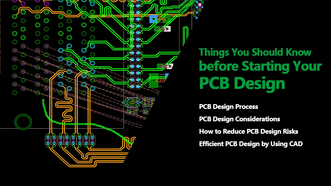
How do you draw pin grid array in cadsoft Eagle PCB?

I'd like to use a processor that uses a pin grid array. Basically, I'd like to make the prototyping PCB board for it. I'm new to eagle. How can I connect the inner PGA pins to the header pins on the edge (without shorting the lines)?

Try not to make so long because your outer pinout is sensible. you should be able to do most of this on one layer. With a standard 5 mil trace/space process, you should have no problem fitting a trace between two pads. It should be possible to route that whole thing on one layer.

Read More: PCB Design Service

#PCB Design
Picture of Oliver Smith

Oliver Smith

Oliver is an experienced electronics engineer skilled in PCB design, analog circuits, embedded systems, and prototyping. His deep knowledge spans schematic capture, firmware coding, simulation, layout, testing, and troubleshooting. Oliver excels at taking projects from concept to mass production using his electrical design talents and mechanical aptitude.

What Others Are Asking

How can I handle missing solder mask opening on PCB footprint?

I have three through-hole PCBs that are missing front and back solder mask openings for two of the components. The solder mask (usually green) is covering the front and back solder pads. All other pads for all other parts are exposed. Is there a good way to remove the solder mask so that I can solder the components to the board?

Read Detailed Advice From Blog Articles

Scroll to Top