PCB etching is a key procedure in the PCB manufacturing process, its purpose is to remove unnecessary copper from the board. This creates the required circuit pattern that connects the different components on the PCB. Etching a PCB is not an easy task, especially for green hands, as it involves using specific materials, tools, and expertise. Therefore, I want to write this guide to introduce PCB etching in detail, covering the definition, different methods of etching PCB board, and precautions during the circuit board etching process.
What Is PCB Etching?
PCB etching is a manufacturing process used to create the desired copper patterns and circuits on the PCB board. It involves selectively removing unwanted copper from a copper-clad substrate, leaving behind the required copper traces and connections that form the electronic pathways on the PCB.
How to Etch a PCB Board?
To etch a PCB, there are several methods, and the most common method is through the use of a chemical solution, we also call this method wet etching.
Wet Etching
Wet etching usually uses two types of chemicals: acidic chemicals and alkaline chemicals, collectively known as PCB etching solutions.
- Alkaline etching
Alkaline etching refers to using an alkaline PCB etching solution to remove unwanted copper from the PCB board through a chemical reaction. In this process, the PCB is soaked in the solution, and then you need to wait for a while for the solution to fully react with the PCB, and finally the copper is removed. Compared to other PCB etching solutions, alkaline etching is less toxic and more environmentally friendly.
- Acidic etching
Like alkaline etching, acidic etching removes copper through a chemical reaction by soaking the board in circuit board etching solutions. The difference is that the solutions are acidic such as ferric chloride and cupric chloride. And when the etching is complete, the PCB undergoes thorough washing and drying to eliminate any residual acidic solution. The acidic etching method is well-suited for the inner layers of PCBs, as the acidic solutions do not harm the required copper components.
Dry Etching
Unlike wet etching, dry etching uses gas or plasma to remove copper. Below we will introduce two commonly used dry circuit board etching methods:
- PCB laser etching
Laser etching leverages computer-controlled systems to achieve high-precision results. In this process, a concentrated laser beam is used to engrave and remove the unwanted copper traces from the PCB substrate, guided by the digital circuit design data. Unlike wet etching methods that require time to wait for a chemical reaction, laser etching allows for faster production.
- Plasma etching
Plasma etching has very high accuracy, which is difficult to achieve with traditional wet etching. This etching method primarily uses a controlled flow of ionized gas molecules called plasma to etch away unwanted copper from the PCB surface. This technology gives manufacturers a high degree of control and selectivity, so it is suitable for intricate circuit designs and patterns
The Process of PCB Etching Solution
The PCB etching process involves several key steps:
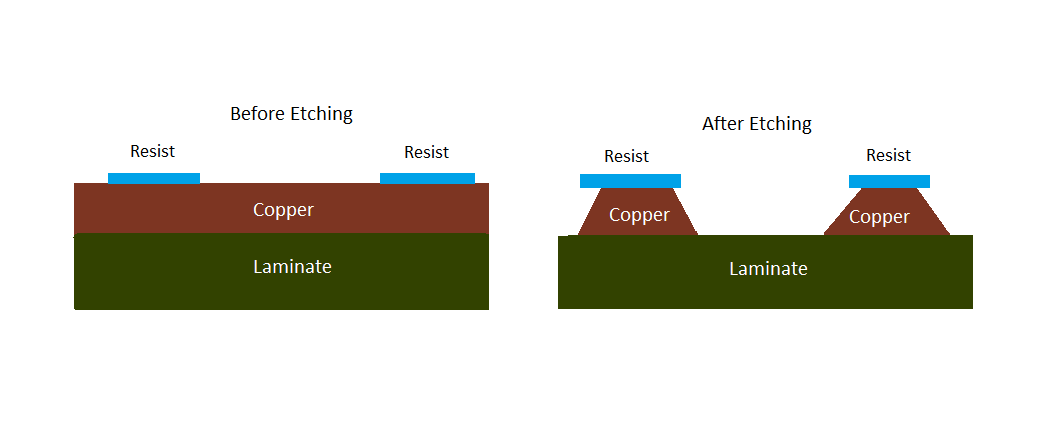
- Surface Preparation
Before etching the PCB board, we must carefully clean the circuit board to remove contaminants such as dust and oil. Otherwise, they can interfere with the etching process.
- Apply Etch Resist
For areas that do not need to be etched, a layer of resist material needs to be applied or printed to protect the copper traces. Common resists are dry film, liquid photoimageable solder mask, and toner.
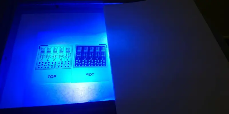
- Expose and Develop Resist
When using light-sensitive resists, the next step involves exposing the PCB to ultraviolet radiation through a patterned mask or artwork film. This UV exposure causes the resist to become hardened and cured in the exposed areas. Then, the board is treated with a chemical developing solution, which dissolves and removes any resist material that was not cured, retaining only the hardened resist that forms the intended pattern on the PCB surface.
- Etch Unwanted Copper
Submerge the bare PCB in an etching solution, which eliminates the exposed copper while preserving the copper traces shielded by the resist, resulting in the formation of the intended circuit patterns on the PCB.
- Remove Resist
Last, we need to remove the remaining resist material to expose the finished copper circuit pattern on the board. This can be done using chemical stripping, abrasion, or thermal methods.
Safety Measures for PCB Etching Processes
Safety measures must be taken when using wet etching because the process requires the use of chemicals. If not properly protected, there will be certain dangers. Below we have listed some suggestions to help you complete circuit board etching safely:
- Wear personal protective equipment, including protective gloves, glasses, and a respirator or mask. Also consider wearing long-sleeved clothing to cover exposed skin. Avoid direct skin contact with solution.
- It is best to perform chemical etching in a well-ventilated environment. Because the etching solution will release steam or smoke, there is a risk of poisoning if inhaled bypeoplein a closed space.
- After the etching process is complete, properly dispose of the used etching solution and any contaminated materials according to local regulations and guidelines.
Final Thoughts
Ensuring the success of circuit board etching is not a simple task; it requires professional knowledge and tools. Whether employing wet etching techniques or opting for advanced dry etching methods, adhering to proper safety protocols and quality control measures is paramount. At MOKO Technology, we understand the intricacies involved in PCB etching and fabrication. Our expertise allows us to deliver premium-quality circuit boards tailored to your specific requirements. Want to start your PCB fabrication project now? Reach out to us to get a free consultation.