People expect electronic products to be rich in functions, but also require them to be small and portable, which brings new challenges to circuit board designers. To achieve this, designers turn to multilayer PCBs, which offer increased space for more signals and electronic circuits to enable greater functionality. However, successful PCB design hinges on careful consideration of the PCB stackup. This critical component directly impacts the circuit board’s performance, reliability, cost, and manufacturability. In this article, you will find guidance on PCB stackup design, including rules, suggestions, and examples to help you complete your stackup design better.
What Is PCB Stackup?
PCB stackup refers to the arrangement of copper and insulating layers that constitute a printed circuit board. A typical PCB stackup consists of alternating layers of copper and insulating material, such as prepreg and core layers. The copper layers contain the circuitry and serve as the conductive pathways for the electronic signals on the board.
The PCB stackup is an essential aspect of the board’s design and determines the electrical properties of the board, including signal integrity, power distribution, and electromagnetic compatibility (EMC). It also impacts the mechanical and thermal properties of the board. The number of layers used in a PCB stackup can be flexible and is determined by the complexity of the circuit and the specific design prerequisites.
A two-layer PCB stackup is the simplest and most common, but high-density designs may require four or more layers to accommodate the necessary components and routing. Designers must carefully consider the PCB stackup during the design process to ensure that the board meets the necessary electrical and mechanical requirements while also being cost-effective to manufacture. Proper stackup design can help minimize signal loss, reduce electromagnetic interference, and provide a stable power distribution network, resulting in a more reliable and high-performance circuit board.
PCB Stackup Design Rules and Tips
Managing a good stackup requires following hundreds of rules and criteria, but some of the most important ones are:
- Ground plane boards are the preferred option as they allow signal routing in either microstrip or stripline configurations, resulting in lowerground impedance and ground noise levels.
- To prevent radiation from high-speed signals, it’s important to route them on intermediate layers between different levels, while using ground planes as shields.
- Signal layers should be placed as close as possible to each other, even if they’re on adjacent planes, and always next to a plane.
- Having multiple ground planes is beneficial as it lowers the board’s ground impedance and reduces radiation.
- It’s crucial to have a strong coupling between power and ground planes.
- A cross-section is advisable from a mechanical perspective to avoid deformations.
- If the signal levels are next to the plane levels, either ground or power, the return current may flow through the adjacent plane, which helps to reduce the inductance of the return path.
- To improve noise and EMI performance, a doable way is to reduce the thickness of the insulation between a signal layer and its neighboring plane.
- When choosing materials based on their electrical, mechanical, and thermal properties, it’s crucial to consider the thickness of each signal layer, taking into account standard thicknesses and the characteristics of various types of printed circuit materials.
- High-quality software should be used to design the stackup, selecting the appropriate materials from the library and performing impedance calculations based on their dimensions.
Recommended Material and Thickness
The three primary components of a PCB stackup are copper, insulation, and ground plane. And the material options and thickness for each of them play a critical role in determining its performance characteristics.
- Copper Layers
There are multiple types of copper available, each with its own unique melting temperature, electrical conductivity, and thermal expansion rate. The selection of copper is typically based on the design requirements. It is worth noting that thicker copper layers improve the overall robustness of the design, but also increase the cost of the board.
- Insulation Layers
FR-4 epoxy, glass epoxy, and parylene-coated materials are the most frequently used types of insulating materials in PCBs. And choosing the appropriate insulation materials is dependent on the application environment. To enhance the EMI shielding and improve the durability of the board, it’s advisable to use an insulation layer that is as thick as possible. However, if the insulation layer is too thick, it may impact the quality of traces and vias.
- Ground Plane Layers
Copper and nickel are the most widely used ground plane materials. The selection of ground plane materials is based on design requirements and the type of solder mask. The recommended thickness for the ground plane is between 0.1 mm and 0.25 mm. Although a thicker ground plane yields better performance, it also leads to an increase in the size of the board.
PCB Stackup Design Examples
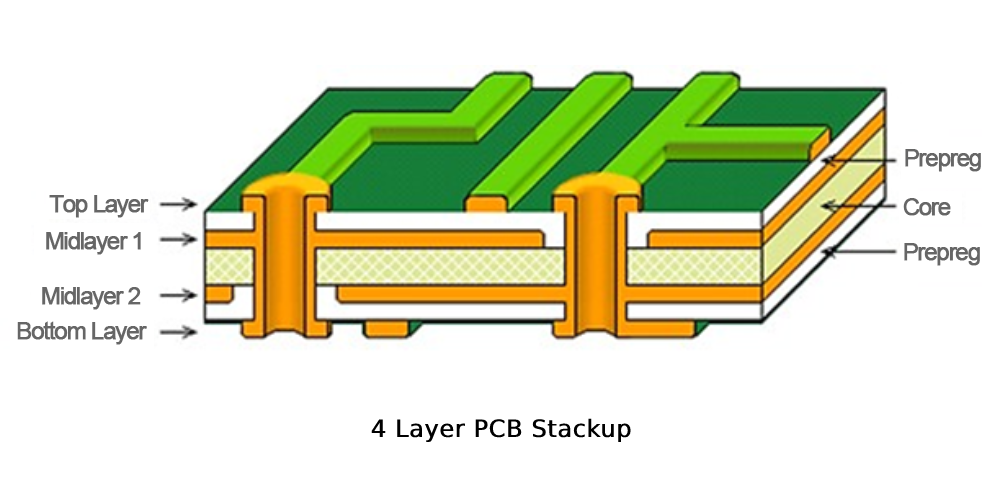
4 layer PCB stackup
A standard 4-layer PCB stack-up typically features a thick core layer in the center of the board, surrounded by two thinner prepreg layers, with the surface layers used primarily for signals and component mounting. The inner layers are often dedicated to power and ground nets. Through-hole vias are commonly used to provide connections between the layers. Solder mask with exposed pads is applied to the outer layers to enable the mounting of SMD and through-hole components.
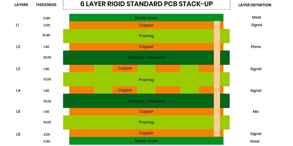
6 layer PCB stackup
The design of a 6-layer PCB stack-up is comparable to that of a 4-layer design, but it has two additional signal layers placed between the planes, resulting in two buried layers that are ideal for high-speed signals and two surface layers that are suitable for routing low-speed signals. Placing the signal layers close to their adjacent planes and using a thicker center core to achieve the desired board thickness (e.g., 62 MIL) can greatly improve EMI performance.
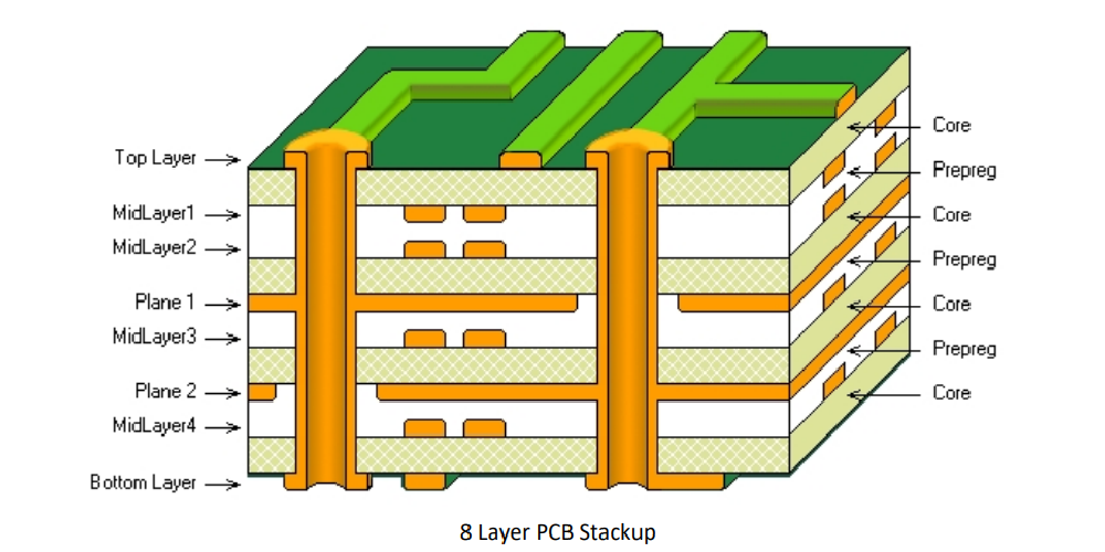
8 layer PCB stackup
For an 8-layer PCB stack-up, the design should include at least three power/ground planes to increase electromagnetic compatibility (EMC) and minimize EMI-related issues. PCB engineers and designers typically consider the circuit’s requirements when designing the stack-up arrangement.
Conclusion
PCB stack-up design is a crucial aspect for both electronic engineers and designers. In order to produce high-quality electronics, various factors must be taken into account. Without a well-designed PCB stack-up, the quality and performance of the final product may be greatly compromised. Therefore, it is important for designers to carefully select the appropriate PCB materials and construction for optimal results. If you lack expertise in PCB stack-up design, consider working with a PCB design specialist. The PCB team at MOKO Technology has extensive experience in designing complex stack-ups, including multilayer and HDI stack-ups. We can assist you in designing a cost-effective and manufacturable stack-up that meets all electrical requirements.