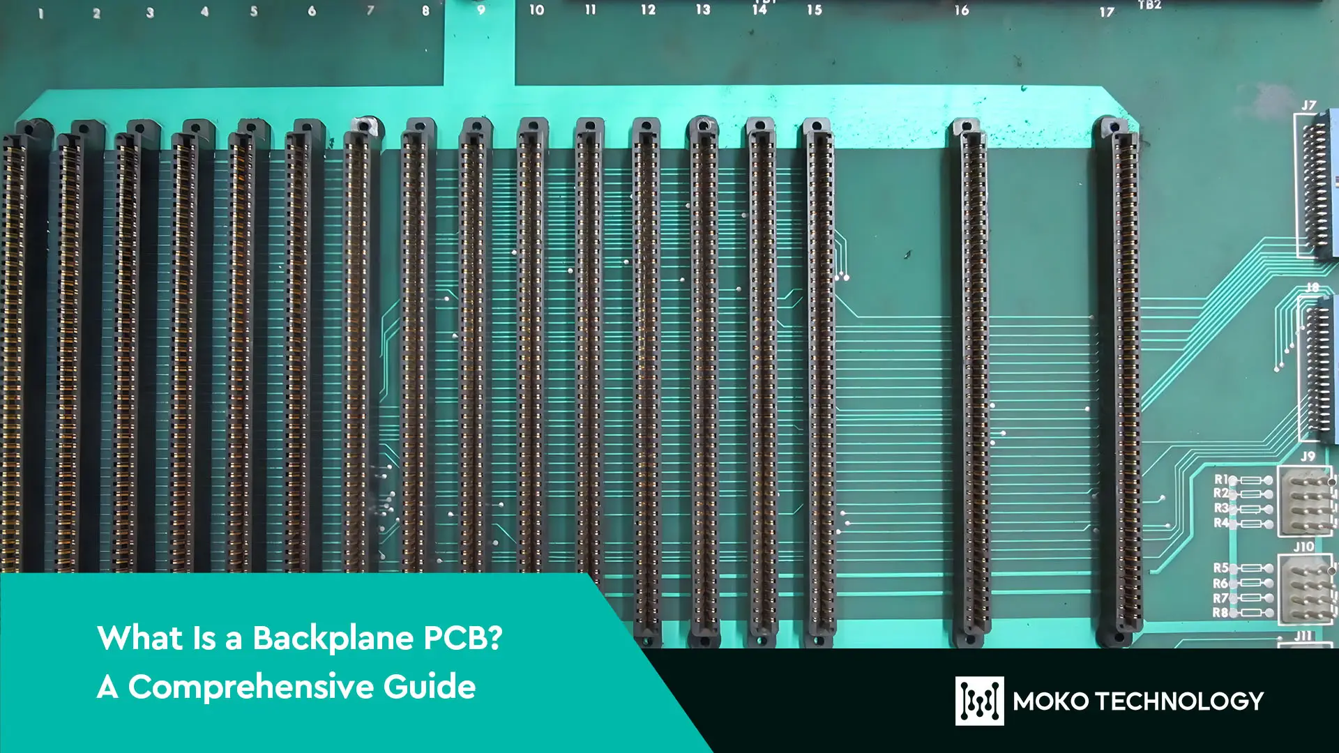
Backplane PCB is the high-speed backbone that turns complex computing and communication systems into realities. They are specialized circuit boards that act as central interconnects allowing several printed circuit boards or modules to be interconnected in terms of their physical and electrical infrastructure. Designing backplane PCBs has now become more critical due to increasing data rates as well as bandwidth requirements. This article gives an insight into in depth aspects of backplane PCBs including their features, advantages, design considerations, and manufacturing difficulties.
What Is a Backplane PCB?
A backplane PCB is a type of circuit board that acts as the backbone or central connecting point for other PCBs or electronic components in the system. The basic idea of the backplane PCB is to offer a physical and electric infrastructure for the interconnection of many printed circuit boards, usually through connectors or slots. It acts as a central bus or communication channel, allowing different boards or modules to communicate with other boards and communicate with each other.
The backplane would normally hold a set of connectors, slots, and sockets for the addition of many modules, otherwise known as daughter cards. These modules may appear as CPUs, memory modules, input/output cards, or other forms of devices.
Key Features of Backplane Printed Circuit Boards
High Density of Interconnections: Backplanes tend to have a higher density of connection because they have many conductive traces on them that link to multiple boards or modules on one or more levels.
High-Speed Data Transmission: High-speed data transfer is the main function of a backplane circuit board as it supports effective and reliable communication necessary for processing large amounts of data at fast rates in any system.
Signal Integrity and Power Distribution: Backplane printed circuit boards guarantee signal integrity so that there is reduced chance of signal loss due to interference while they may also transmit energy effectively guaranteeing a perfect power supply to the daughter boards connected to them.
Backplane Vs. Motherboard: What’s the difference?
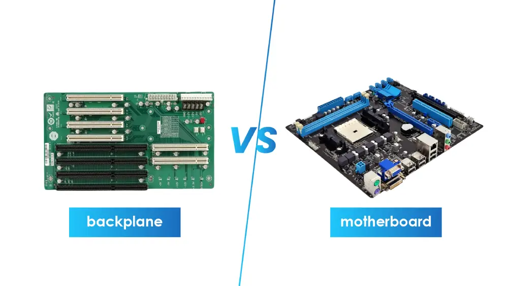
Although a backplane and motherboard do have some similarities to each other in being central circuit boards for electronic systems, they really differ in their prime functions and design considerations. A backplane mainly acts as a high-speed interconnect for a number of removable boards or modules; it can be thought of as a centralized communication hub. On the other hand, a motherboard is developed to host and integrate various crucial components like a CPU, memory, and expansion slots, which form the core of a computer system. The design of backplanes normally considers high-speed signal integrity, power distribution, and modular scalability, while that of motherboards includes integration and compatibility among the components in a system architecture.
Challenges in Backplane PCB Manufacturing
- PCB Thickness: In backplanes, controlling thickness is difficult; thickness must increase to ensure matched impedance and signal integrity in these backplanes due to the need for controlled impedance transmission lines, power planes, and return paths.
- High Layer Count: Usually, high numbers of layers (e.g. 20) characterize backplanes as a means of accommodating interconnected circuitry. This creates challenges in layer registration, via alignment, and pressing.
- Complexity in Drilling: The thickness of the backplanes means that larger drill diameters and higher aspect ratios are required, requiring multiple drill passes for a single via—something that is bound to affect the accuracy of the drilling and yield. Further reading: PCB Drilling: Everything You Need to Know Is Here
- They have a need of exact impedance match in case of high-speed data transmission which is difficult to attain due to different dielectric materials and connector interfaces.
- For the backplane performance and reliability, high densities of connectors require precise connectors alignment as well as signal integrity.
How to Design Backplane PCB?
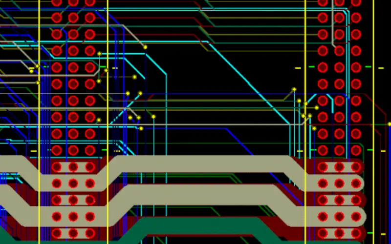
Designing a high-performance backplane PCB requires focusing on two key aspects: electrical design and mechanical design. Below, we list the key considerations for each aspect:
Electrical Design
Power Delivery: Ensure stable and clean power supply by following a robust power distribution network consists of thick power/ground layers and ample decoupling capacitors near connectors.
Layer Structure:
Use a high number of layers (20+) with multiple signal-return layer pairs. Each pair should use identical dielectric materials and dielectric thicknesses for impedance management.
Signal Routing: To achieve target impedance, we should match trace widths and spacings during backplane PCB design, also routing critical signals on inner layers adjacent to reference layers is needed.
Component Placement: Correctly placing components, such as bypass capacitors, termination resistors, and active devices close to connectors, can ensure signal integrity.
Mechanical Design
Card Support: Card support involves specifying accurate card guides, slots and stiffeners to assist in ensuring the right insertion of cards as well as holding them, while also preventing the board from bending due to weight.
Connector Mounting: When mounting connectors, particularly using connectors rated for numerous mating cycles, the application of heavy-duty press-fit connectors or soldered connectors together with necessary footprints and stiff supports at its back is necessary to limit its bending during insertion and removal.
Thermal Management: Ensure sufficient airflow channels, use thermally conductive dielectric materials, and use thermal pads/vias underneath hot devices.
Advantages of Using Backplane PCBs
Simplified Interconnectivity: Backplane PCB acts like a central hub which helps to simplify connection between different circuit boards or modules. This role prevents intricate webs of cables being formed by multiple connectors thus easing assembly process as well as reducing chances for signal loss and improving overall systems’ safety.
Scalable Flexibility: Backplanes are made with many slots or connectors to accommodate new components or to upgrade the system without making huge changes. Such scalability makes backplane PCBs an economically feasible and flexible option for electronic systems that may need additional enhancements.
Improved Signal Integrity: These specialized PCBs provide a controlled and stable environment for signal transmission, thus significantly minimizing opportunities for signal distortion, crosstalk as well as EMI related disorders that have the potential to reduce system performance of electronics.
Space Optimization: Due to the consolidation of interconnections onto a single backplane, there is alleviation in bulky and complex wiring, effecting substantial space savings within the system. This is particularly useful in systems with small physical sizes or those that demand high portability.
Conclusion
We have seen from the text above that backplane PCBs enable powerful computing systems and communication devices which are central to our modern life. They enable high speed communication while interconnecting several circuit boards and modules effectively. Moreover, they are involved in space management and scalability that makes these devices practical. Hope this blog can provide insights to help you better understand this important technology. And if you still have other questions about the backplane, contact us to explore together!