Complete Guide about Multilayer PCB
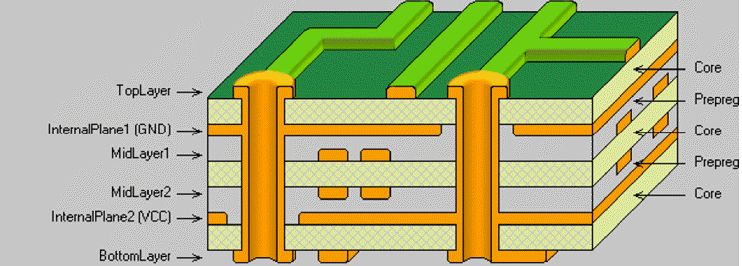
Multilayer PCB is a type of circuit board that contains three or more layers of conductive material. These boards increase the available area for wiring. Whenever we talk about a number of layers, it means we are considering a number of conducting patterns on the board. Multilayer PCBs are normally Rigid PCB. It is because it is very difficult to create it in a flexible format.
The number of layers depends on your needs. So layers could be up to 100. However, 4 to 8 layer PCBs have common usage in various applications. Circuitry gets complex when layers increase. So you can customize different numbers of layers according to your needs.
Different essential components of multilayer PCB
There are 4 main components of multilayer PCB as follows:
- Substrate: it is the most important part usually made of fiberglass. Fiberglass provides the core strength to the PCB and resists against breakage. You can consider the substrate as a skeleton of PCB.
- Copper layer: It depends on the board type. So this layer can be either full-on copper or a copper foil. Regardless of the board type, the copper layer is still the same. So copper carries electrical signals to and from the PCBs. You can consider this layer as a nervous system. That carries signals from the brain to your muscles and vice versa.
- Solder Mask: It is a layer of polymer that protects the copper layer. So it basically prevents short-circuit when copper comes into contact with the environment. So you can consider the solder mask as the skin of the PCB.
- Silkscreen: It is the final part of the PCB. The silkscreen basically shows part number, symbols, and logos of different components on the board. Furthermore, it also provides information like symbols switch settings, test points, and component references.
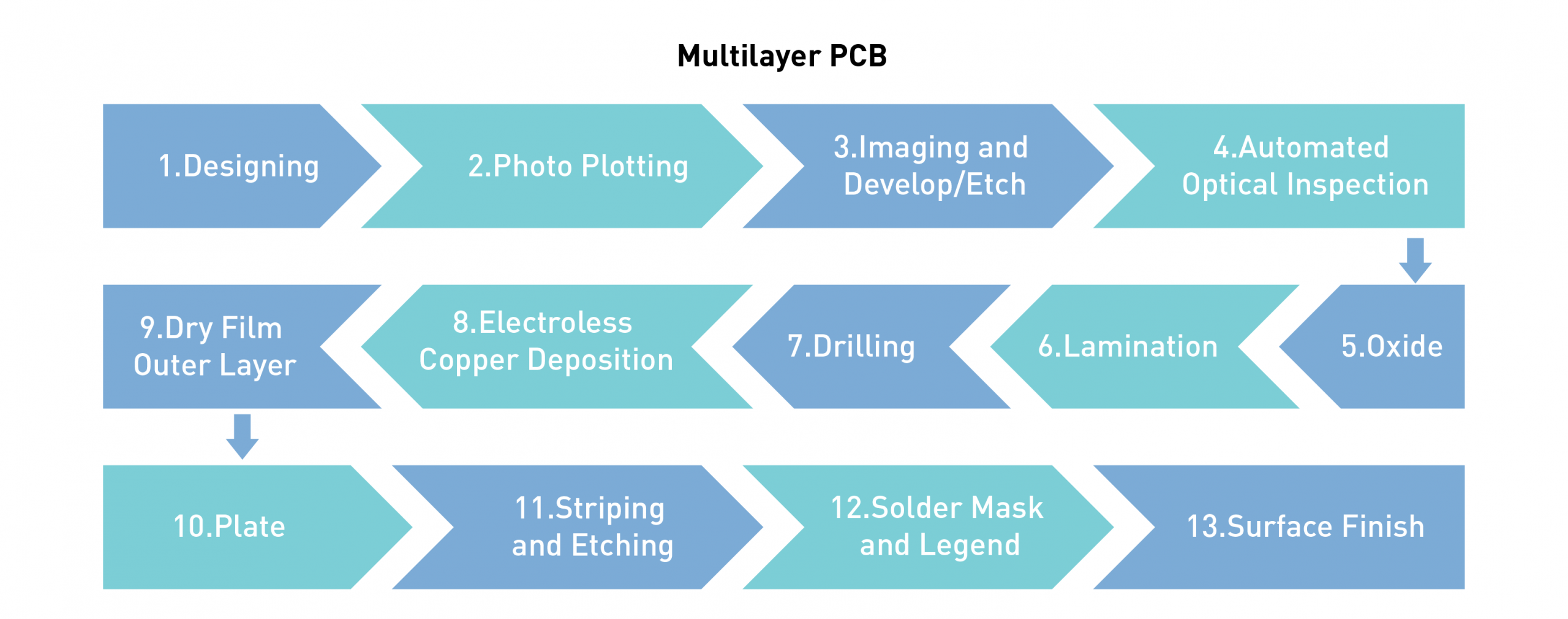
How to manufacture Multilayer PCB?
Here is the complete step by step guide for manufacturing multilayer PCB:
Designing
The first and foremost step to design PCB and prepare them for production. All manufacturers have their own approach to this process. Generally, the designer lays out a blueprint for the circuitry and fulfills all the outlined requirements. Different types of software are available for designing such as Extended Gerber.
So you can use Extended Gerber or any other tool to design your circuit. Once you design the circuit, carefully check the entire design. Make sure that there is no error in the entire blueprint. After designing, you can send this blueprint to the fabrication house to start building circuitry.
Photo Plotting
In this step, you can use a laser photo-plotter to plot a film for each individual layer. A laser photo-plotter is a tool used to create photo-tools for solder mask and silkscreen. The thickness of the film is about 7 mils.
Many manufacturers use special laser direct imaging equipment that images straightly onto the Dry Film. This technique reduces costs. Furthermore, the process is more accurate and effective. So you can produce internal as well as external layers using laser direct imaging (LSI).
Imaging and Develop or Etch
This process applies the primary images such as pads and traces onto the circuit board. Besides this, the DES process creates the copper pattern for the plating. Here is what to do in this step:
- Apply photo imageable to the copper panels.
- Furthermore, image the panels using LSI.
- Etch off the whole exposed copper from the panel.
- Strip the remaining Dry Film and just leave the remaining copper pattern for the inner layers.
Automated Optical Inspection
AOI basically inspects different layers of multilayer PCB before laminating all layers together. The optics compare the PCB design data to the actual image on the panel. Any differences such as missing or extra copper can result in opens or shorts. So this process basically helps manufacturers to catch any defect in the circuitry.
Oxide
Oxide is a chemical treatment to inner layers before lamination for multi-layer PCBs. Moreover, the oxide code is brown or black depends on the process. It is an important step to increase the roughness of copper to enhance the laminate bond strength. Furthermore, this process prevents the separation between different layers of the base material.
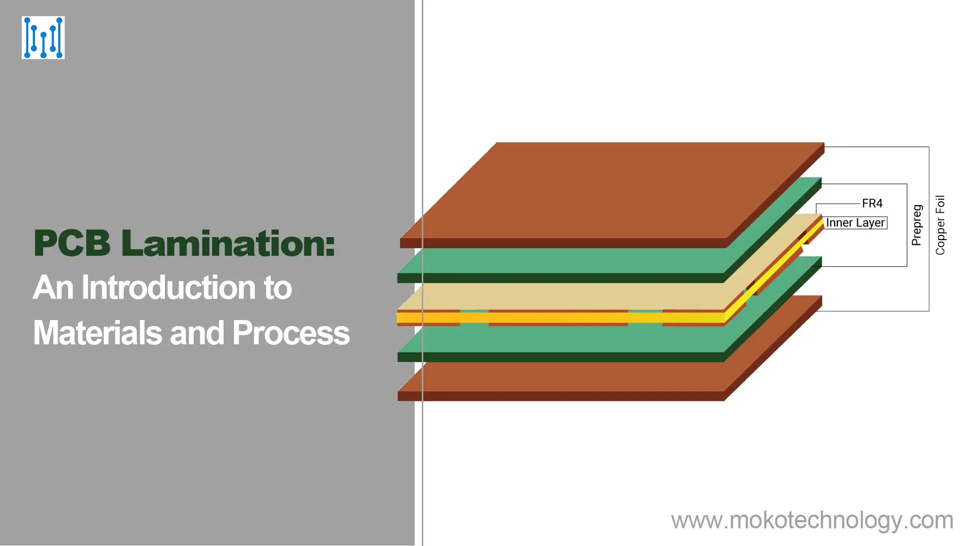
Lamination
To produce a multilayer PCB, different layers of epoxy-infused fiberglass are laminated together. For lamination, manufacturers apply high temperature and pressure using a hydraulic press. The presser and heat cause the fiberglass sheet to melt and tightly join the layers together. After cooling this material, it further follows the same manufacturing process as a double-sided PCB.
Drilling
All PCBs need some holes to link copper layers, attaching components and mounting the PCB. So you can drill holes using some advanced drilling systems. These systems use solid carbide cutting tools. Furthermore, these have a design for the fast removal of chips in abrasive materials.
A pre-programmed drill machine drills specific-sized holes at the exact location. So the drill machine works according to the designer’s provided data. Designers provide this information as a numerically controlled drill file.
In addition to this, a thin sheet of aluminum acts entry material. Besides this, hard cardboard acts as exit material. So this technique keeps the drilling smooth and avoids creating different fibers.
Electroless Copper Deposition
After drilling, manufacturers deposit a thin coat of copper on the exposed surfaces of the panels chemically. Furthermore, they deposit a copper coat on the hole walls using electroless plating.
Dry Film Outer Layer
After copper deposition, you must apply the outer layer images to prepare the panel for electroplate. So you can utilize a laminator machine to coat outer layers with the dry film. The dry film is a photo imageable material. Moreover, this process is almost similar to image the inner layers of a multilayer PCB.
Plate
The electroplating process involves copper plating onto the conductive pattern. Plus on the hole walls of the PCB as well. The thickness of the plating is around 1 mil. After copper plating, you need to deposit a thin layer of tin plating. The tin plating layer serves as an etch barrier.
Striping and Etching
After completing the plating process on the panel, the dry film remains. But you need to remove the copper that lies beneath. Now the panel will go through the SES process. So SES stands for String Etch Strip.
In this process, you need to etch the exposed copper. It means you will remove the uncovered area of copper by tin. So traces and the pads around the holes and copper patterns remain there. At last, you will remove the remaining tin that is covering holes and traces chemically. So after completing this step, you only leave behind exposed laminate and copper of the PCB.
At this stage, the skeleton of the PCB is complete now. Now all onwards steps are related to protecting PCB.
Solder Mask and Legend
Most manufacturers use a liquid photo imageable (LPI) Solder mask to protect the copper surface. It further protects solder bridging between different components during assembly.
LPI solder mask is basically a photo-sensitive epoxy-based resist. You can cover the entire panel by using the screen printing process. There are some other alternative methods to the traditional screen plating. So you can use such an alternative for solder masking.
After the solder mask, you can apply legend. It prints different symbols and letters on the PCB for reference during assembly.
Surface Finish
It is the last and final chemical process to manufacture a multilayer printed circuit board. Solder mask covers almost all circuitry. So the surface finish prevents oxidation of the remaining exposed copper area.
This is an important step because you cannot solder the oxidized-coper. Furthermore, you can use different types of surface finish for this step. Such as you can you hot air solder level (HASL).
The benefit of multilayer PCB
Here are some advantages of multilayer PCB over other types:
- It has a higher assembly density than single and double-layer PCBs.
- There is no need for cables to interconnect different components. So it is an ideal choice for low weight PCBs.
- These PCBs come in smaller sizes resulting in reduced space requirements.
- EMI shielding is straightforward and flexible.
- Flexibility is another factor that stands out multilayer PCB among all printed circuit boards.
Different applications of multilayer PCB
Many electronic components use a multilayer PCB. Moreover, these circuits encompass intermediate to complex range of circuitry structure. Here are some significant applications of multilayer PCB:
- Heart Monitors
- Cell phone transmission and repeaters
- Atomic accelerators
- Space probe and X-ray equipment
- Weather analysis and GPS technology
- Data storage and file servers
- Fiber optic receptors and Cat scan technology
How to identify a multilayer PCB
If you have some PCBs and want to check the total number of layers, you can follow these steps.
Expose the edge of the circuit board to the light to see the copper planes. So in this way, you can easily watch trances more closely. Even if the multilayer PCBs don’t contain blind via, you can still utilize bright light to analyze the inner layers.
The best place to detect the inner layers is where no path and lines visible on the outer layers. Moreover, the majority of manufacturers print the label to identify the total number of a layer on the circuit board. So by just looking at the edges, you can identify the total number of layers.