What’s the thickness of FR4 substrate that one should take when designing a micro-strip antenna with an HFSS tool?

I am designing a micro-strip antenna with an HFSS toll, what's the thickness of FR4 substrate that one should take ?

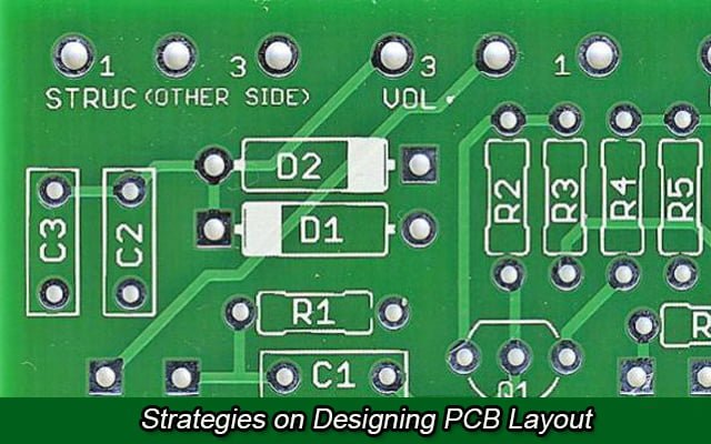
As I recall, most FR4 stock is .062in thick. The thickness of the stock is not quite as important as to your specification of the stock.

One can have a PCB house plate copper onto the standard board stock to your specs, which might be more useful in your micro-strip design parameter selection.

To be fair, though, I am unfamiliar with the software tool you mentioned. I had to do the design the hard way and tweak as necessary.

Remark:

  • If the board is single-sided, then the above is true. The copper thickness is more important than the substrate itself.
  • If one is using a two-sided, or multilayered design, the thickness of the stock is one more difficulty to be solved in designing your micro-strip elements., especially the distance to a ground plane.

Read More: How to Choose the Right PCB Thickness?

#PCB Design #PCB Materials

Picture of Oliver Smith

Oliver Smith

Oliver is an experienced electronics engineer skilled in PCB design, analog circuits, embedded systems, and prototyping. His deep knowledge spans schematic capture, firmware coding, simulation, layout, testing, and troubleshooting. Oliver excels at taking projects from concept to mass production using his electrical design talents and mechanical aptitude.

What Others Are Asking

How much larger should a plated-through hole be than lead diameter to get good solder wetting?

I’m designing a new PCB where I have a whack of connectors that have to line up with the metalwork. There are some problematic connectors. All 4 pins are round. I want to have the holes as small as possible while allowing for good solder adhesion over the full length of the pin. I’m looking for guidance on how much clearance around the component lead I should have in order to get good solder wetting and adhesion.

Is saving through-hole components viable?

I recently got my hands on some old electronics. After getting some to work and failing to get others to work. My Question-Is desoldering and salvaging through-hole and surface-mount PCB components viable, or should I just buy the components online?

Read Detailed Advice From Blog Articles

Strategies on Designing PCB Layout
Ryan Chan

Strategies on Designing PCB Layout

Why PCB Layout is Needed We use Printed Circuit Boards (PCB) for connecting electronic components by using conductive tracks. This allows for prototyping electric circuits

Will Li

A Comprehensive Guide to PCB Prepreg

Prepreg, short for pre-impregnated composite fibers, is an essential material in the manufacture of multilayer printed circuit boards. However, it is often overlooked compared to more visible

Scroll to Top