PCB thickness is one of the important factors to consider when manufacturing printed circuit boards, it affects the conductivity, resistance, and performance of the PCB. In the PCB industry, there is no uniform standard for PCB thickness, but there are some thicknesses that are preferred and commonly used by many manufacturers. These thicknesses can therefore simplify design, minimize cost and shorten turnaround times. Then, according to the specific needs of the customer project, the thickness of the PCB can also be customized, and the thickness of the PCB can be changed in the design stage to adapt to the specific manufacturing purpose and final application. In this blog, we explain standard PCB thicknesses, list the key factors that affect PCB thickness, and finally, we provide some insights on how to choose the right PCB thickness for your project.
What Is the Standard PCB Thickness?
It is considered that 1.57 millimeters(approximately 0.062 inches) is the standard PCB thickness by many manufacturers, primarily because this was the size of bakelite boards made in the early days of the board manufacturing process and has remained constant throughout. However, today’s board sizes have more options, and depending on the end application, they can be manufactured larger or smaller than this standard, so it is more accurate to say that there is a range of common or standard PCB thicknesses. In addition to 0.062-inch boards, 0.031-inch and 0.093-inch boards are commonly used, and these sizes meet the needs of more robust or multi-layer boards.
Key Factors Affect the Thickness of PCB
- Copper Thickness
The overall thickness of a PCB can be influenced by the thickness of the copper layers it contains. Thicker copper layers, such as 2 oz (ounce) or 3 oz copper, will contribute more to the overall thickness compared to thinner copper layers like 1 oz copper. And the thickness of the copper layer used is decided by the current that needs to pass through the circuit boards.
- Substrate Material
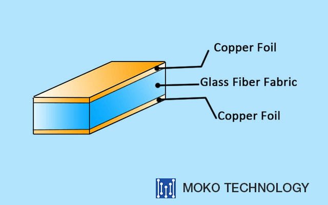
The choice of substrate material can significantly impact PCB thickness. Different materials have different thicknesses, for example, the substrate of flexible printed circuit boards tends to be thinner compared to rigid PCB substrates. Common substrate materials like FR-4 have standard thicknesses, but specialized materials may have unique thickness characteristics.
- Number of PCB layers
For single-layer PCBs, they have a smaller thickness compared to multilayer printed circuit boards. The standard threshold of PCB thickness typically accommodates 2-6 layer PCBs. However, for PCBs with 8 layers or more, the thickness may not fall within the standard range. Each additional layer adds to the overall thickness of the PCB.
- Signal Types
The thickness of PCBs is influenced by the types of signals they carry. For instance, PCBs carrying high power signals necessitate thicker copper layers and wider traces, resulting in a significantly thicker board compared to those operating in low power environments. On the other hand, high-density boards with complex signals often utilize laser microvias, thin traces, and thin high-performance materials, making them traditionally thinner than other types of boards.
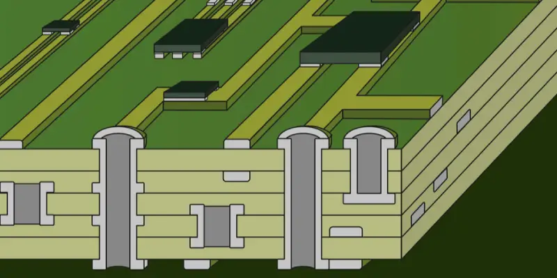
- Types of Vias
PCB vias play are essential for routing traces across different layers of the board, enabling more compact and efficient designs. Various via types are available for different applications, including through via, micro via, blind via, and buried via.
The selection and density of vias used in a PCB design will influence the required board thickness. For example, utilizing micro vias on thinner PCB boards is feasible because they are smaller in size and well-suited for high-density connections. Understanding the characteristics and limitations of different via types is essential in determining the appropriate PCB thickness for a given design.
- Operating Condition
Operating condition is another important factor that impacts the PCB thickness. For instance, in challenging operating conditions, such as rugged environments, a thin or flexible board may not be the most appropriate choice. Similarly, thicker copper traces are less thermally stable when exposed to high currents, which makes them less ideal for environments with variable temperatures or high currents.
- Depanelization Method
Depanelization plays a crucial role in determining the thickness of PCBs during manufacturing. Manufacturers typically produce PCBs in large panels that contain multiple boards, which are later separated into individual units. The thickness of the board influences the depanelization methods employed. Thicker boards may require careful scoring for separation, while thinner boards can be routed to create breakaway tabs.
Top Considerations When Custom PCB Thickness
Weight: Thicker boards are generally preferred over thinner ones, as thinner boards tend to be more brittle and prone to breakage unless the specific application necessitates a thin board.
Flexibility: Thin boards offer greater flexibility compared to thick boards, but they are also more susceptible to breaking. Thick boards, on the other hand, are less flexible but heavier.
Space Constraints: The size of the device and the available space for accommodating the PCB will influence the choice of board thickness. Larger devices can accommodate thicker boards, while smaller devices require smaller boards.
Connectors and Components: The type of connectors and components used in the PCB design may have specific thickness requirements that need to be considered.
Impedance: The thickness of the board directly relates to the thickness of the dielectric material used, which plays a significant role in achieving proper impedance characteristics. By ensuring that the board thickness matches the intended impedance, optimal signal integrity and performance can be achieved in the PCB.
Manufacturing Equipment Capability: It is important to ensure that your chosen PCB manufacturer possesses the necessary equipment to produce the desired board thickness.
Extended Turnaround Time: Uncommon PCB thicknesses may involve longer lead times to acquire. It is crucial to take into account the potential impact on the quality of development and the timeliness of delivery.
Additional Costs: Evaluate the additional costs associated with special materials, manufacturing processes, and potential loss of man-hours to determine if the added expenses are acceptable.
Final Thoughts
Choosing the standard PCB thickness is generally a cost-effective and efficient option for manufacturing your boards. It allows for faster production and is readily available from most manufacturers. However, if your application requires specific functionality and unique requirements, opting for a custom thickness may be necessary. In such cases, it is crucial to ensure that your chosen PCB manufacturer has the capabilities to accommodate your specific thickness needs.
MOKO Technology is a leading PCB supplier in China, with nearly 20 years of experience, we are capable of manufacturing a wide array of printed circuit boards, providing one-stop PCB solutions ranging from PCB design, and manufacture to PCB assembly and testing. Our flexible and strong capabilities allow us to manufacture PCB with standard and customized thicknesses to better suit your project requirements.