Why do newer devices lack external antennas?

  • Technology got better: sensitivity increased, antenna design got better so patch antennas (integrated with PCB or integrated with the case) became not just practical but universal.
  • The second technology reason is probably an aspect that antennas have become much more complex: multiple bands, MIMO, etc. As a result, it is important they are aligned just so, and placed carefully. Patch antennas fixed at manufacture make that practicable.


  • From a consumer perspective, antennas were not necessary most of the time anyway. Famously, there was one model of cellphone (a Motorola I think) that did not have an external antenna in Europe or Asia (where they were considered ugly & old-fashioned) – but did have in the USA because that was what the market required, because they were considered better.
  •  Of course, it would have been really hard (electrical design, PCB layout, RF testing, EMC compliance) to actually have two designs – so the US market had an ‘antenna; which was a plastic fake; the rest of the world had exactly the same phone but no fake plastic antenna.


Read More: How to Design PCB Antenna Like a Pro?

#PCB Assembly #PCB Design
Picture of Oliver Smith

Oliver Smith

Oliver is an experienced electronics engineer skilled in PCB design, analog circuits, embedded systems, and prototyping. His deep knowledge spans schematic capture, firmware coding, simulation, layout, testing, and troubleshooting. Oliver excels at taking projects from concept to mass production using his electrical design talents and mechanical aptitude.

What Others Are Asking

How much larger should a plated-through hole be than lead diameter to get good solder wetting?

I’m designing a new PCB where I have a whack of connectors that have to line up with the metalwork. There are some problematic connectors. All 4 pins are round. I want to have the holes as small as possible while allowing for good solder adhesion over the full length of the pin. I’m looking for guidance on how much clearance around the component lead I should have in order to get good solder wetting and adhesion.

Is solder mask a valid electrical insulator?

There is a copper pour over the entire top of the my PCB, which is part of GND net. It turns out that the surface mounted 1W LEDs I’m going to use have the heat slug connected internally to the LED’s +ve terminal. Can I rely on the solder mask to insulate the +ve voltage (~3V ish) from GND? Long term?

Read Detailed Advice From Blog Articles

A Brief Guide to Prototype PCB Assembly
Will Li

A Brief Guide to Prototype PCB Assembly

What Is Prototype PCB Assembly? Prototype PCB assembly refers to the experimental phase that follows the PCB design to demonstrate the feasibility of the design

best practices of rigid flex pcb
Ryan Chan

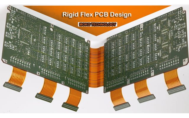
Best Practices of Rigid Flex PCB Design

Rigid Flex PCB Design: Benefits and Design Best Practices With the use of a rigid flex PCB(rigid FPC), flexible circuit substrates and rigid circuit substrates

Strategies on Designing PCB Layout
Ryan Chan

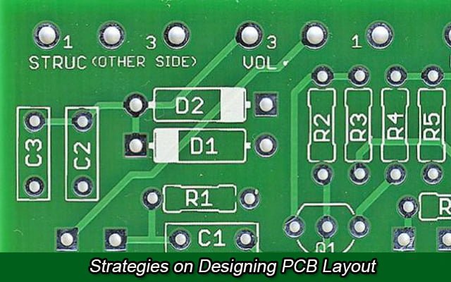
Strategies on Designing PCB Layout

Why PCB Layout is Needed We use Printed Circuit Boards (PCB) for connecting electronic components by using conductive tracks. This allows for prototyping electric circuits

Scroll to Top