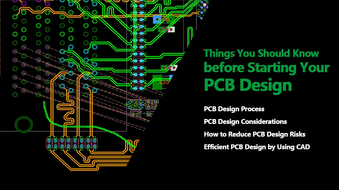
Approximately how many PCB layers would be needed to route a 1088 pin BGA IC?

I am designing a PCB with 1088 pin BGA IC. Haven’t handle such a big IC. I am not sure the best amount of layer.
  • Remember that ALL of the power pins, Vcc, GND, others can be tied to a single layer.
  • If there isneed for video or other analog signals, then you need a layer for ANLG and AGND. That should reduce the pin counts.
  • If there are address and data buses, those signals can be restrained to their own layers as first. Their physical lengths may need to be restrained to their own layers at first as well.
  • Critical traces, such as clocks or other high-speed traces should never run parallel to non-high-speed traces or other clocks. Some of these can be run on extra ground plane layers.
  • Also, ensure your PCB manufacturer can handle your project. I once had a 14-layer prototype PCB catch on fire due to reduced Pre-preg thickness to meet the mechanical fit.

Read More: IC Package Types: How to Choose the Right One?

#PCB Design
Picture of Oliver Smith

Oliver Smith

Oliver is an experienced electronics engineer skilled in PCB design, analog circuits, embedded systems, and prototyping. His deep knowledge spans schematic capture, firmware coding, simulation, layout, testing, and troubleshooting. Oliver excels at taking projects from concept to mass production using his electrical design talents and mechanical aptitude.

What Others Are Asking

How can I handle missing solder mask opening on PCB footprint?

I have three through-hole PCBs that are missing front and back solder mask openings for two of the components. The solder mask (usually green) is covering the front and back solder pads. All other pads for all other parts are exposed. Is there a good way to remove the solder mask so that I can solder the components to the board?

How do I determine the traces width when designing a PCB?

Our team are developing a portable medical device with a small size, so we need a small PCB. How do I determine the traces width when designing a PCB? Actually we want it as narrow as possible to fit the device, is it OK?

Is paste mask layer, both top and bottom layer, necessary for THT components?

I know the paste mask layer is also called the stencil layer. It’s only used for assembly. I want to know if the paste mask layer (both top and bottom layer) is necessary for through hole components. For SMD components I know the paste mask layer is required to solder the components. Is it necessary for through hole components?

Read Detailed Advice From Blog Articles

Scroll to Top