The designer places marks on copper layer for easy identification after the artwork is prepared. Part number on the copper layer will last till the PCB lasts itself.
#PCB Design

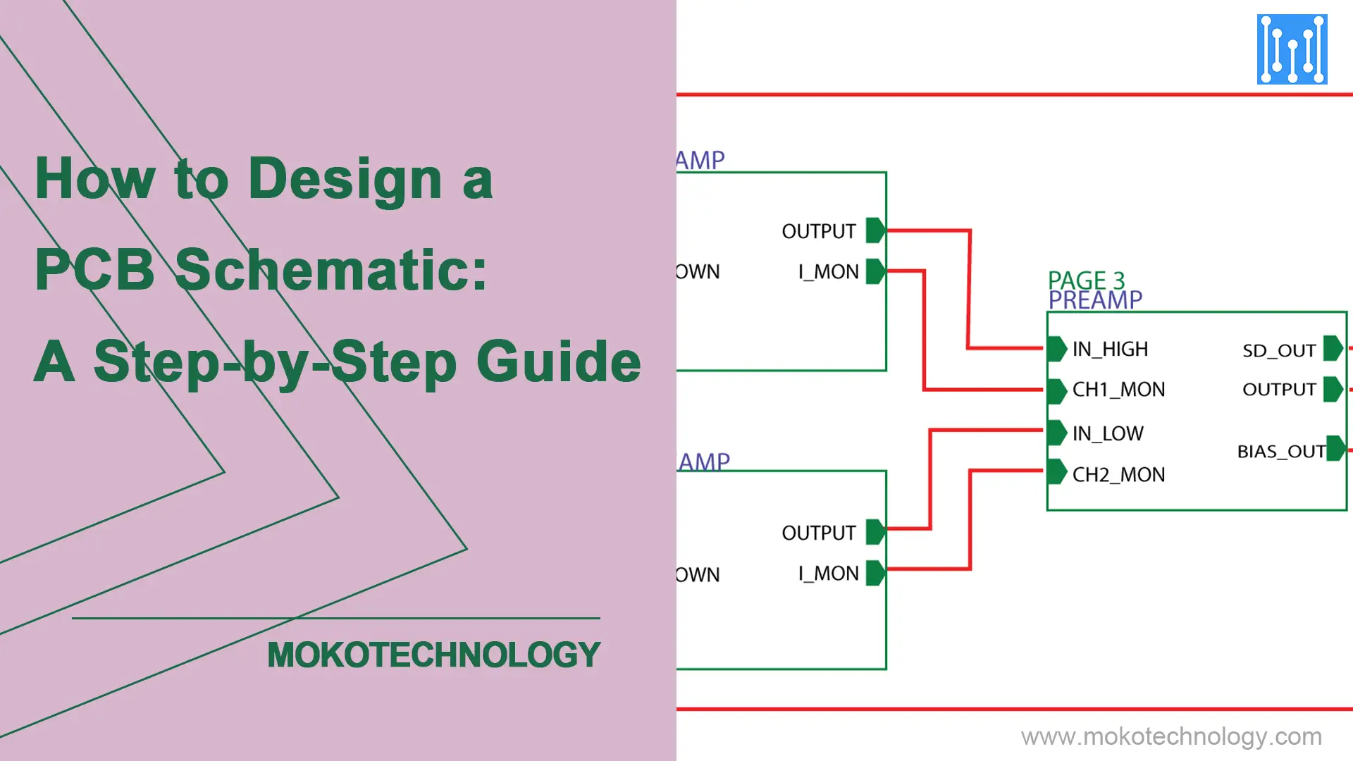
PCB Schematic: What Is It? Why Is It Important? A printed circuit board design starts with a PCB schematic diagram. This PCB schematic layout visually depicts the
PCB layout design is a key step in the manufacture of circuit boards. A reasonable PCB layout is conducive to controlling the production cost and
Printed circuit boards with high-speed chips and microwave PCB structures have numerous parameters that differ significantly from those of conventional, rigid and flexible printed circuit
