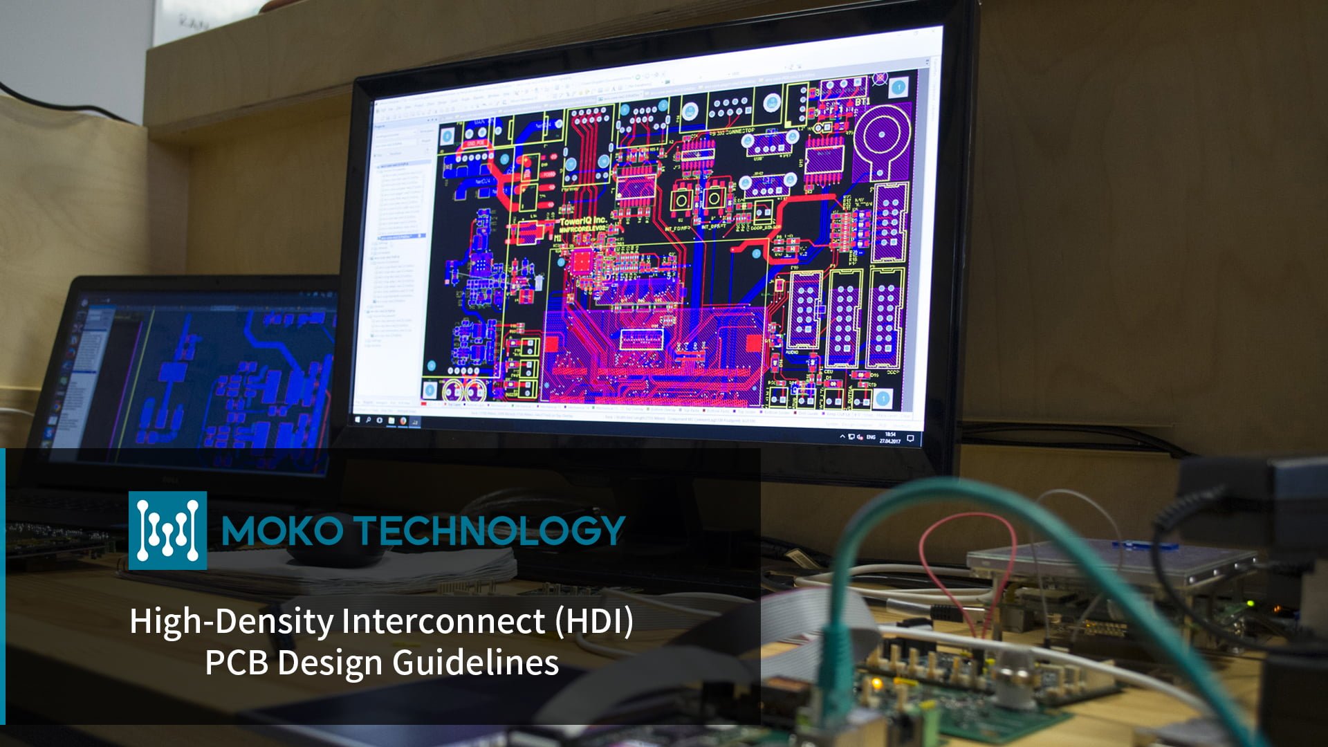
You are here because you want to learn about high frequency PCB design. This guide explains in detail different factors having an influence on high frequency PCB. Furthermore, we will discuss different challenges to this type of PCB and solution as well. In short, this comprehensive guide expresses everything you need to know regarding high-frequency PCB design.
High frequency PCB is a type of PCB that have wide usage in different applications such as microwave. So let’s dive in and try to explore different incredible aspects of this technology.
High Frequency PCB
Most of you are familiar with the word PCB. If you are not, it is basically an acronym of the Printed Circuit Board. So PCB uses conductive tracks and paths to connect different components on the circuit board electronically. Copper is the main substance of PCB that provides a conductive path on the board.
In addition to this, signal communication plays a key role in different electronic projects. For example, it is crucial in those projects where Wi-Fi and satellite systems involve. So when there is a need for signal communication between two or more objects, high frequency boards come in usage.
So high frequency PCB is a type of circuit board used for signal transmission. For example, companies use it in the microwave, mobile, radiofrequency and high-speed design applications.
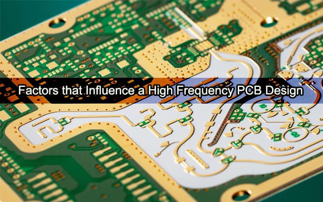
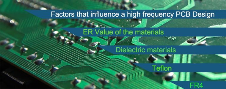
Factors that influence a high frequency PCB Design
There are some important factors that have a high impact on high frequency PCB design. So these boards come with high frequency laminates, that are difficult to fabricate. It is because they need to maintain the thermal heat transfer of different applications.
Circuit boards use special materials to attain a high frequency. So characteristics of the high frequency board affect the overall performance of the signal. Furthermore, a slight change in the ER value of the materials can have an impact on the impedance of the board.
Besides above all, dielectric materials also influence a high frequency PCB design. Most of the manufacturers prefer rogers dielectric material. This material is less expensive and it has low DK and DF value as well. Furthermore, it appears to be suitable for prototyping applications and fabrication. In addition, it also reduces signal loss as well.
On the other hand, some manufacturers go with Teflon. Manufacturers use it in high frequency board manufacturing. Moreover, it basically comes with 5 GHz frequency. Moreover, FR4 is another popular material used for RF applications. The applications require 1 GHz to 10 GHz frequency use FR4. However, FR4 based products have their own limitations and drawback.
So in terms of DF, DK and water absorption factor, Teflon is the finest option. However, it is more expensive than FR4. If your project requires more than 10 GHz frequency, Teflon is the best choice.
General specification of high frequency PCB
To achieve high frequency for your needs, you can use different special materials. Furthermore, any change in the Er value of different materials can have a significant impact on the impedance of the board. You can find PCBs with different frequencies. So the typical range of frequency from 500 MHz to 2 GHz.
However, let’s discuss some generic specification of high frequency PCB:
- Material: RO4003C, Ro3003, RT5880 and Ro3010
- Board Size: Min 6mm x 6 mm or max 457 mm x 610 mm
- PP: Rogers 4450F, Domestic-25FR, Domestic-6700
- Board Thickness: 4 mm to 5.0 mm
- Copper Weight: 5oz to 2.0oz
- Solder Mask Sides: As per the file
- Solder Mask Color: Green, Blue, Red, White, and Yellow
- Min Tracking or Spacing: 3mil/ 3mil
- Silkscreen Sides: As per the file
- Silkscreen Color: Black, White, and Yellow
- Surface Finish: Electroless nickel/ immersion gold, immersion silver, immersion tin –RoHS
- Impedance Tolerance: Plus or Minus 10%
- Min Drilling Hole Diameter: 6mil
- Min Annular Ring: 4 mil
If you want to purchase the best quality high frequency PCB, MOKO Technology is the best option. You can customize these circuit boards according to your needs. For a consultation, you can contact the professional team of MOKO Technology.
How to identify the best high frequency PCB?
It is not a big deal to identify the high frequency PCB. Look at the general specification and the material used to construct PCBs. So you can identify the high frequency PCB. Otherwise, if you are not familiar, you can consult any trustworthy company such as MOKO Technology.
Different useful tips of high frequency PCB design and manufacture
High frequency circuits have a higher layout density and higher integration. So it is crucial to know how to design and manufacture more reasonable and more scientific circuit boards. Let’s have a look some of the most useful tips:
- It is better to have the less alternative leads of the pins between different layers of high frequency circuits.
- There should be a shorter lead between the pins.
- It is important to have less bend between the pins of high frequency electronic devices.
- Try to avoid loops while wiring.
- Make sure to have good signal impedance matching.
- Furthermore, you should increase the high frequency decoupling capacity of the power pins of an integrated circuit block.
The challenge of high frequency PCB design and how to encounter it
During the manufacturing process, you can face different challenges. Below is a brief overview of some common challenges:
Scaling
Most circuit board fabricators are familiar with the concept of artwork scaling. As internal layers lose some mass during the lamination process while building FR4 multilayers PCBs. So it is important to scale-up circuitry by known percentage in anticipation of this loss. So the layers return to their as-designed dimensions after the completion of the lamination cycle.
Moreover, laminate materials behave somewhat differently because of being softer than FR4. However, the idea is almost similar to figure out what the material is likely to do. As it goes through the process. It means you should establish separate scale factors for each type. Furthermore, you should create a separate scale for each thickness within a single type even.
Otherwise, registration from layer to layer or drill to pad can be compromised. The fabricator should use the baseline scaling recommendation of the laminate manufacturer with an in-house statistical process. So it will be consistent over time within the special manufacturing environment.
Surface Preparation
Multilayer surface preparation is complex for getting a secure bond between layers. So it is specifically true for Teflon types. Therefore, the soft material can be deformed if the preparation is very aggressive. So significant deformation can lead to poor registration. In addition to this, if the deformation is quite obvious, PCB may end up as a non-functional scrap.
Deburring can actually polish the substrate. This can affect adhesion in multilayers. It is because some materials contain pure Teflon. So this product is renowned for its non-stick nature. To replace this material can be costly and result in long delays as well. The only way to avoid such an outcome is to carefully perform this step. So make sure to perform this step correctly.
Hole Preparation
Before plating through with copper, you must remove surface irregularities. You should further remove debris and epoxy smear. As a result, the plating will adhere to the hole walls. RF materials such as ceramic or PTFE/ Teflon need different ways for hole preparation.
In this process, try to adjust different drill machine parameters to prevent the substrate from smearing in the first place. During the hole treatment after drilling, the plasma cycle uses various gases from normal boards. If you fail to prepare the holes before plating, interconnection will be poor. That will fail over time. So it is important to form clean holes for long-term reliability.
Thermal Expansion Rates
CTE is another crucial factor for long-term reliability. CTE stands for the coefficient of thermal expansion. Manufacturers use it to measure the amount of expansion of different materials. Expansion can go in any of the three axes under thermal stress. If the CTE is lower, the less likely the plated holes will fail from repeated flexing of the copper.
Furthermore, CTE can be complex if you combine high frequency materials with FR4 in hybrid multilayer PCB constructions. It is because the CTE of one material must match with the other materials. Otherwise, different layers will expand at different rates that can be problematic.
In addition to layers, the same is true for vias as well. So material used for plugging vias should match the other materials as well in the stack. So before manufacturing high frequency PCB design, you should consider this important factor.
Machining
There are some RF materials that behave very similar to the FR4 laminates while machining. So it is very important to understand some basic differences. For instance, ceramic-impregnated types can be very hard while drilling through on drill bits. So it is very important to reduce maximum hit counts. Moreover, you should customize spindle infeed and RPM settings.
Fibers can also remain inside hole walls. So these can be very difficult to remove. So try to adjust drilling parameters so that fiber occurrence should be minimized.