If you want to control currents for electrical drives and power supplies with intelligent electronics, you have to master the balancing act between power and microelectronics. This article describes different variants of a unique and diverse high current PCB technology that are suitable for currents up to 1,000 A. At the heart of this technology are embedded copper bars that protrude from the surface to contact SMDs and other power components.
In order to close the gap between high-current conductors on the one hand and electronic components on the other, a number of cables, mounting materials, and interposers are usually required, especially if SMDs are provided. The aim is to integrate busbars in printed circuit boards in order to save construction volume and assembly effort for systems and to combine the drive and supply currents as well as electronic controls.
There are a number of circuit board technologies that are designed for power applications. These include multilayers with increased copper layer thicknesses of up to 400 micrometers, which can be leveled at higher layers. In addition, several techniques are offered that rely on a selective increase in the copper cross-section, such as the iceberg technique, the wire laid technique and the partial embedding of thick copper laminates.
Drive technology: Optimize high current PCB for motor controls
Three PCB technologies for high-current circuit boards are compared in this article: Dickschicht, Iceberg, and HSMtec. PCB topology and PCB design influence the current carrying capacity and heat dissipation of the power semiconductors.
Suitable technologies are available for combining the load circuit and fine conductor for logic signals on an FR4 circuit board. You save space and avoid the conventional connection technology with separate boards, which increases the reliability of the motor control. The PCB developer can optimize the current carrying capacity and heat dissipation of the power semiconductors according to his task.
From the point of view of the printed circuit board, the specifications of the drive electronics can be summarized in five points: 1) high integration density, 2) reliability of the electronic assembly, 3) fast heat dissipation, 4) high currents combined with control electronics and 5) reduced system costs, e.g. by switching to SMD components, fewer components or assembly processes.
A smart solution is to combine the power section and the control electronics, i.e. the load circuits and the control logic, instead of on two circuit boards on just one circuit board. However, this requires large conductor cross-sections and large insulation distances for the high-current conductors and, at the same time, fine conductor structures for the control on one and the same board. This eliminates expensive plug connections, cables, and busbars, as well as assembly steps and risks that limit reliability. The PCB specialist KSG has three technologies for this: thick copper, iceberg and HSMtec technology. All three processes use the standard base material FR4.
Safe contact with high current PCB
All of these technologies have something in common: There is usually not a sufficient cross-section between the layers of the high current PCB board and the connections for surface-mounted components or screw connections. The vias form a bottleneck for the currents of the desired size. And the press-in plugs, screws, and clamps also do not guarantee reliable contact with the layers. Only the clean soldering of connections forms a continuous connection from the components to all layers. Here, however, the higher the total copper thickness, the riskier is the solder penetration.
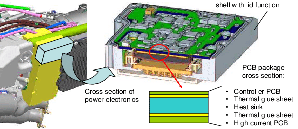
In contrast, regardless of the design, the high-current circuit board contacts the components and connections with the maximum conductor cross-section (Figure 2 below). In this way, SM and THT components can be combined with bonded power semiconductors, press-in contacts and screw connections without a bottleneck in the current path. At the same time, the busbar serves as a heat sink. The components are in direct contact with this thermal mass and are therefore optimally cooled.
Design, production, and processing of high current PCB
Compared to conventional busbars known from electrical engineering, individually shaped copper parts are used for the high-current circuit board. The shape and position of the copper parts can be freely defined. This gives the layout designer the freedom to place the components and connections in such a way that a compact module with optimized thermal and electrical functions is created.
Since each high-current project has its own characteristics, it is difficult to lay down general design rules. Depending on the size and shape of the copper parts and insulation bars, the design limits for each project must be checked. Guideline values provide a rough guide for the design.
To manufacture a high current PCB circuit board, the copper parts are first manufactured. Depending on the size, shape, and number of parts, this is done by etching, milling or punching. The copper parts are placed in pre-milled frames and then pressed with prepregs and possibly other layers.
One advantage of the high current PCB is the processing. Because the busbars are embedded, the high-current circuit board – apart from its weight – cannot be distinguished externally from other circuit boards. It can be processed in conventional SMD processes if the profile is set to the higher thermal mass. Experience shows that these soldering processes can be mastered well. A repair process for components that come into direct contact with the high-current rail, on the other hand, is more complex than with conventional flat assemblies.
Technology variants of high current PCB
The full potential of the high current PCB board becomes clear when you consider the possible variations.
The technology offers the greatest benefit if the copper parts are shaped in such a way that they reach the surface and are flush with the other pads on TOP and / or BOT (Fig. 1). This gives you a completely flat circuit board that can be further processed in the subsequent paste printing and assembly process without adjustment. Cable lugs, modules, and screwable components are also easier to connect to the high-current position.
In another version of the technology, the high current layer protrudes laterally from the edge of the circuit board. These contacts can be used directly as plugs or can be contacted like the end of a conventional busbar.
The next two variants of the high current PCB circuit board aimless at high currents than at cooling components.
If the copper parts have SMD connection surfaces both upwards and downwards, they work like conventional printed circuit board inlays, which are pressed into the cutouts in printed circuit boards to conduct heat from power components from TOP to BOT. The embedded copper parts (Fig. 9) differ from conventional inlays in that they are more reliable in manufacture and processing since there is no mechanical stress on the circuit board. In addition, the size and position of the pads can be selected independently of one another. An electrical connection is also possible without additional effort.
The last variant of the high current PCB board is a one-sided version (Figures 10 and 11). Here, raised pads of copper sheet protrude through the insulation of a thin insulation layer, in order to then be contacted directly as SMD heatsink contacts to the corresponding component connections. In contrast to aluminum substrates made from IMS, this version does not have an insulation layer, so that significantly higher powers can be dissipated here. Such constructions are used, among other things, for high-performance LEDs with up to 10 W.
With the high-current circuit board, MOKO Technology is expanding its range of technologies in the field of thermal management with another important component:
Solid copper is embedded in the circuit board and can be fitted directly to SMD pads that reach the surface.
Structure of an SMD high-current circuit board
The high current circuit board can also be contacted with other assembly and connection technologies:
– Reflow/wave soldering SMD / THT- Aluminum wire bonding
– Screws: eyelets / threaded holes
– Blind holes from the outer layers
– Press-fit technology high current connector
In many cases, the additional effort for the production of high current PCB can be reduced partly through specially implemented manufacturing processes and partly through optimized process control of standard processes.
Thick copper PCBs distribute the power losses horizontally
Thick copper technology has been established on the market for many years and is manufactured in large quantities. The PCB industry usually speaks of thick copper for copper structures of ≥105 µm. Thick copper conductors serve the better horizontal heat distribution of high power losses from power components and/or for the transport of high currents and replace stamped and bent constructions for busbars in high current PCB applications. With up to four inner layers, each with 400 µm copper, a current-carrying capacity of several hundred amperes is possible. Ideally, the thick copper conductors are located in the inner layers.
Flexibility for changes in the layout, the compact design, simple processing/assembly and comparably low change costs as well as the standard processes of the PCB industry speak in favor of the thick copper PCB. Although the process steps of a thick copper circuit board do not differ significantly from the standard throughput of a conventional circuit board, the production requires special process experience and management. A thick copper circuit board stays in the etching line 10 to 15 times longer and has a typical etching profile. The etching and drilling processes of the thick copper circuit board determine the design rules for the circuit diagram and must be observed. The PCB manufacturer has a list of suggestions for cost and process-optimized layer construction and design rules.
Important to know: FR4 laminates with a base copper cladding ≥105 µm are more expensive due to the high copper content. Compared to a standard laminate laminated on both sides with 18 µm, the material cost factor is around 1: 8 to 1:10. The PCB developer must pay attention to maximum material utilization. Early coordination with the PCB manufacturer helps to significantly reduce costs. With regard to miniaturization, thick copper technology is limited. Due to the strong undercut, only relatively coarse structures can be created. Another limitation: fine signal wiring is not possible on the same wiring level as the thick copper conductor.
Iceberg: for a uniform surface topography
In a wiring level, there are areas with 70 to 100 µm copper for the logic and areas with up to 400 µm copper for the load. The thick copper is largely sunk in the circuit board. This creates a uniform surface topography across the entire conductor pattern. The iceberg principle can also be combined with thick copper on the inner layers.
Embedding two-thirds of the 400 µm thick copper area in the base material creates a planar printed circuit board surface. Advantage: The conductor flanks can be reliably covered with a solder mask in just one casting process. The subsequent assembly process is possible on one level. Iceberg structures are also suitable as heat sinks for power components and can be combined with plated-through holes (vias) to optimize thermal management.
HSMtec: copper elements in the inner and outer layers
Another way to combine load and logic on a circuit board is HSMtec. Here, massive copper elements are selectively installed in the inner layers and under the outer layers of the FR4 multilayer at those points where high currents flow, and ultrasonically bonded to the base copper of the etched conductor patterns. After pressing the layers, the copper profiles are located under the outer layers and/or in the inner layers of the multilayer. The rest of the circuit board remains unaffected.
The multilayer is manufactured in the standard manufacturing process and further processed in the usual assembly and soldering process. With this structure, the electrical specifications for the dielectric strength and insulation classes of machines can be served as well as demanding temperature conditions with limited installation space in vehicles.
The solid copper profiles inside the multilayer also enable three-dimensional constructions. Notch milling perpendicular to the copper profiles allows segments of the circuit board to be bent up to 90 °. In this way, installation space is cleverly used and high current and heat are transported over the bending edge. The construction is laid out as a two-dimensional circuit board, manufactured and assembled in the panel. After assembling or assembling the module, the circuit board is bent into the three-dimensional shape.
The software supports the developers in dimensioning high-current conductor tracks. With just a few entries such as current and temperature, the calculator provides the minimum wire width for HSMtec as well as for 70 and 105 µm copper cladding.