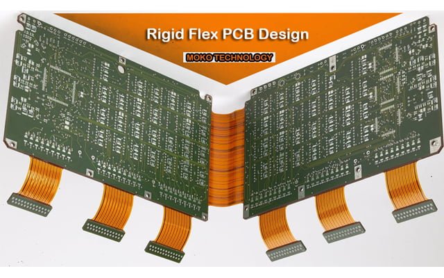
Printed circuit board (PCB) manufacturing typically involves panelizing – grouping multiple PCBs together on a large panel that is then fabricated, assembled, and depanelized. The use of panels provides several advantages compared to manufacturing individual PCBs separately. Optimizing PCB panel size and layout is crucial for maximizing manufacturing efficiency and minimizing costs. This article will provide key tips for utilizing PCB panel size optimally.
What Are Standard PCB Panel Sizes?
There are several standard panel sizes commonly used in PCB fabrication:
18”x12”
18”x24”
9”x24”
9”x12”
These standard PCB panel sizes are widely supported by manufacturing facilities. Using them simplifies logistics and processes compared to custom PCB panel size.
The benefits of using standard panel sizes include:
- Consistent quality and lead times since fabrication equipment is designed for these sizes
- Optimized panel yield
- Cost savings through economies of scale
The tradeoff is that standard sizes limit layout flexibility compared to custom panels, and not all quantities or PCB sizes can be accommodated optimally. As a result, unused space on panels is possible when using standard sizes.
Choosing Between Standard and Custom Panels
Custom panels should be considered when:
- The PCB shape is odd or non-rectangular
- Very high order quantities need to be accommodated
- Maximizing panel utilization is critical
When deciding between standard or custom PCB panel size, factors to consider include :
- Manufacturer capabilities and recommendations
- PCB sizeand order quantity
- Impact on testing and handling procedures
- Effects on routability
- Future volume scaling requirements
Discussing options with your PCB manufacturer can help determine the optimal balance of cost, lead time, and panel utilization. Their expertise can inform the standard vs. custom panel decision.
Tips for Optimizing Panel Utilization
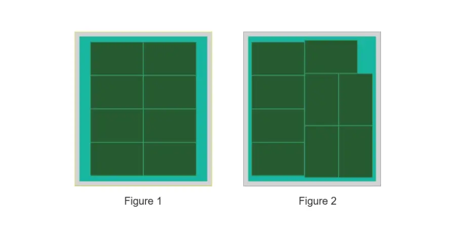
The layout of the PCB panel is critical as it directly impacts panel utilization. For example, below are two different panel layouts with the same PCB panel size of 21″ x 24″.
In Figure 1, there are only 8 PCB boards that can fit on the panel. The boards are all aligned in the same orientation.
In Figure 2, some of the boards have been rotated to optimize spacing. With this improved layout, 9 PCB boards can be placed on the panel.
By rotating and rearranging the board positions, the panel utilization is increased from 64.8% in Figure 1 to 72.9% in Figure 2.
This example illustrates how thoughtful PCB placement and rotation can maximize the number of boards per panel.
In addition to optimized panel layout, there are several other strategies to improve PCB panel utilization:
- Consider Panel Sizes and Spacing
Familiarize yourself with common PCB panel sizes used by suppliers (e.g., 16 x 18, 18 x 24, 21 x 24).
Determine minimum spacing between parts on the panel and minimum panel borders (typically around 0.1″ with 0.75″ panel borders).
- Choose Board Sizes Selectively
When designing your PCB panels, be selective about the sizes of boards you include. As a general guideline, avoid using boards smaller than 75mil x 75mil. Larger board sizes provide adequate space for components and modifications.
- Combining Different Circuit Boards
You can optimize panel space by combining different circuit boards on one panel. Place boards of various sizes but identical thickness on a single panel. Or, arrange a series of PCBs with different layouts on one panel. Either approach allows you to fit more boards per panel by reconfiguring the placement and using different panel sizes.
- Part Size Optimization
Understand how reducing part sizes can increase the number of parts per panel. Perform analyses to find the threshold at which reducing part sizes leads to improved panel utilization.
- Strategically Position Fiducials and Tooling Holes
Carefully plan the location of fiducial marks and tooling holes on the panel. Position them in a way that doesn’t block usable space for PCBs. This ensures you maximize the available area for boards.
- Account for Trim Tolerances
Leave enough tolerance space around the edges of the panel for trimming, drilling rails, and any required fixtures. This prevents accidentally cutting into the PCBs during manufacturing.
- Minimize Irregular Negative Space
When placing PCBs on a panel, position them to minimize irregular negative space between boards. Align board edges where possible to fully utilize the panel area.
- Use Panelization Software
Panelization software allows you to experiment with different PCB placement arrangements to find the optimal layout for your panel. Maintain proper electrical and mechanical clearances between boards.
Conclusion
PCB panel offers many benefits if utilized thoughtfully, following PCB layout and panelization best practices ensures maximum efficiency and cost savings. The small upfront time investment pays dividends across the entire manufacturing process.
Working closely with an expert manufacturing partner for planning panelization is highly recommended. Their guidance can help identify the most suitable panel size and optimize the layout. A reliable partner like MOKO Technology has extensive experience delivering optimized PCB panelization solutions tuned for cost-effectiveness and quality.