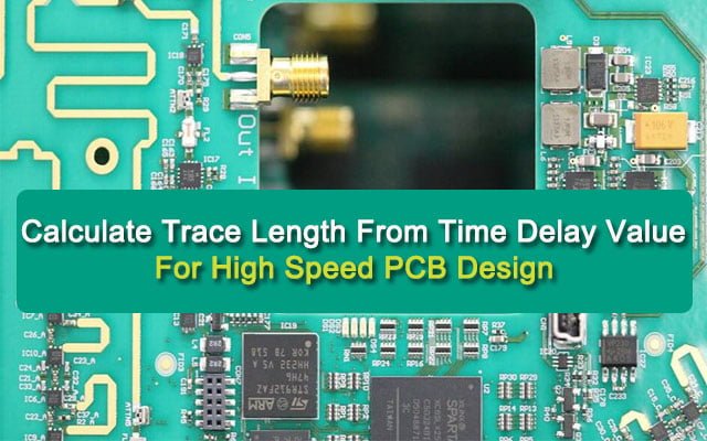
Maintaining high speed PCB design quality from the driver to the collector on the PCB is not an easy task. One of the most testing issues is dealing with the engendering deferral and relative time postpones bungles. To deal with the time delays, we have to realize how to figure follow length from time postpone an incentive to execute the PCB support steering as needs are. Let me show you the procedure. The high-frequency PCB design also requires selective material for PCB.
Finding a high Speed PCB Design
As per material science, swift sign travels in a vacuum or through the air at a similar speed As light, which is.
Looking for high speed PCB design:
According to materials science, electromagnetic signals travel in a vacuum or in the air at a speed similar to that of light, that is:
Vc = 3 x 10⁸ m/s = 186,000 miles/s = 11.8 inches/ns
Due to the influence of the dielectric constant (Er) of the PCB material, the signal passes through the PCB transmission line at a slower speed. In addition, the transmission line structure also affects signal speed.
There are two general PCB follow structures:
- stripline
- microstrip
The equations for computing the sign speed on a high-frequency PCB are given underneath:
Where:
Vc is the speed of light in a vacuum or through the air
Er is the dielectric steady of the PCB material
Ereffis the compelling dielectric consistent for microstrips; it’s worth lies among one and Er, and is roughly given by:
Ereff≈ (0.64 Er+ 0.36) (1c)
Figuring engendering delay (TPD)
The spread deferral is the time a sign takes to increase over a unit length of the transmission line.
Here is how we determine the diffusion delay from the following lengths and other methods:
Where: symbol speed relative to the transmission line
In a vacuum or air, it rises to 85 picoseconds per inch (ps/ In).
On PCB transmission lines, the engendering delay is given by:
How to choose High-Speed PCB Design Material
Before selecting the high-speed PCB material for your fast PCB plan, it is essential to decide a worth (or qualities) for DK and Z0 for your transmission line (or lines). Your high-speed PCB board structure programming may enable you to set these qualities and incorporate them as a component of the plan file(s) for your agreement maker (CM). If not, there are dk outlines and impedance mini-computers online to assist you with landing at the best possible qualities. Presently, you are prepared to actualize the 2-advance answer for your fast PCB structure material choices!
Stage 1: Select board material sorts
Pick material sort from types prescribed for high-recurrence PCBs. This incorporates choosing center, prepreg, and substrate materials. You might have the option to profit by half breed development, where sign layer material is picked for high recurrence. Yet, different layers may utilize different materials to diminish manufacturers’ costs.
Stage 2: Select board material thicknesses and copper loads
Utilize your determined or favored qualities for DK and Z0 to choose thickness and copper loads. Make sure to keep up impedance consistency all through sign ways. Your CM ought to be a piece of your material choice procedure as the board manufacture, and PCB gets together stages may expect adjustments to your determinations before your sheets can be made. Rhythm Automation, the industry head in quick, exact PCB model assembling, is prepared to band together with you and help you in upgrading the material determination process.
Also, to assist you with beginning on the best way, we outfit data for your DFM and empower you to see and download DRC documents effectively. In case you’re an Altium client, you can permanently add these documents to your PCB structure programming.
If you are prepared to have your plan made, attempt our statement device to transfer your CAD and BOM documents. If you need more data on rapid PCB plan or making material determinations for your board, get in touch with us.
Impedance Matching in High-Speed PCB Design
It isn’t predominantly to take a gander at the recurrence, yet the key is to take a gander at the steepness of the edge of the sign, that is, the ascent/fall time of the sign. It is commonly viewed as that if the ascent/fall time of the sign (in 10% to 90%) is under multiple times the wire delay, it is fast. The sign must focus on the issue of impedance coordinating. The wire delay is ordinarily 150ps/inch.
Standard Impedance Matching Method
1. Couple Terminal Matching:
Under the condition that the sign source impedance is lower than the trademark impedance of the transmission line, a resistor R is associated in arrangement between the source end of the sign and the transmission line, so the yield impedance of the source end coordinates the trademark impedance of the transmission line, and the sign reflected from the heap end is stifled. Re-reflection happened.
2. Parallel Terminal Matching:
For the situation where the impedance of the sign source is little, the info impedance of the heap end is coordinated with the trademark impedance of the transmission line by expanding the parallel obstruction, to wipe out the reflection at the heap end. The execution structure is isolated into two
Coordinating obstruction choice guideline: For the situation of a high information impedance of the chip, for a solitary opposition structure, the parallel opposition estimation of the heap terminal must be near or equivalent to the trademark impedance of the transmission line; for the double obstruction structure, each parallel obstruction esteem It is double the trademark impedance of the transmission line.
The benefit of parallel end coordinating is primary and straightforward. The notable drawback is that it will bring DC control utilization: the DC control utilization of the single obstruction mode is firmly identified with the obligation cycle of the sign; the binary opposition mode is whether the symptom is high or low. There is DC control utilization; however, the current is not precisely 50% of the single resistor. Moreover, high-speed PCB design guidelines are enough to guide you.