PCB is a fundamental building block of all electronic components. So it comes with various different types of layers. For a beginner, PCB Layer types and PCB layers boards types can be confusing. However, after having a basic understanding of these concepts, it appears quite simple.
This detailed article explains everything you need to know about PCB layers types and how to optimize them. Let’s come straightly to the points and elaborate on different PCB layers.
Types Of PCB Layers
Mechanical Layers
A single PCB circuit board can have multiple mechanical layers. However, you need at least one layer to fabricate your board. The most common mechanical layers form the physical dimension of your board. This layer assists a fabricator to cut out the circuit board from stock material.
This layer can be a simple rectangle or a complicated shape having round corners or cut-outs. In addition, some mechanical layers contain details tooling specifications and some other mechanical information. These extra mechanical layers have seldom usage so there is no need to dive deeper.
Keep Out Layers
Contrary to the mechanical layers, keep out layers define the constraints of the working area of circuit boards. For instance, if you want to draw all components ½ inch from the perimeter of your board. Then, the keep out layer will come under discussion.
This layer is very helpful to give feedback to the designer. So it assists designers not to violate the predetermined boundaries. Moreover, you can use it to identify segments on the interior that need to stay clear for different reasons.
Routing Layers
Routing layers are very helpful for interconnecting different components. Designers spend most of the time on routing layers for best performance. Routing layers can lie on both inner and outer layers. Moreover, in PCB layers stack up against the world, manufacturers call them as the top or bottom layers. You must provide routing layers to your fabricator while creating circuit boards.
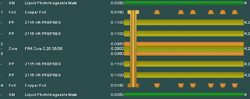
Ground Planes and Power Planes
These are both solid copper layers shorted to a fixed potential. In simple words, you need to connect ground planes to GND and power planes to one of your onboard voltage. Likewise routing layers, these layers can lie as internal or outer layers of PCB.
Both layers are very advantageous for power distribution. Moreover, these are convenient for ground across all of your components. In addition, these can boost the performance of circuitry in certain conditions. You must provide all the files that describe all planes within your design while creating your custom circuit board.
Split Planes
Power and ground planes contain multiple sections of copper connected to different potentials. So you can modify them easily. It is very helpful to enhance the convenience of planes. For example, your plan can have multiple voltages on it distributing +5V to one section and -5V to another section.
There can be some performance issues while dealing with splitting planes up. Performance issues occur most often in the ground plane. Above all, split layers are handy to increase the convenience of planes.
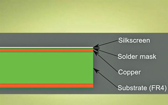
Overlay or Silkscreen Layers
Overlay or silkscreen layers are additional layers to add text for all components on the circuit board. You need to add these layers on both top and bottom layers. If you want to utilize this layer, you need to provide separate layers for both top and bottom overlays.
Although circuit boards work perfectly fine even without these layers. However, you should add this layer to improve readability while repairing your circuit boards. In addition, you can add your company name, design name, serial or revision number of a circuit board. There is no need to add this layer to the internal layers because you can’t see them!
Solder Mask Layers
It is another one of the most common PCB layers types. Circuit boards come in different colors like green and blue. So the thin colored protective covering of the PCB on the top and bottom is solder mask. Solder mask plays an important role to protect traces from shorting when the debris is present on your board.
Solder mask is not mandatory for manufacturing PCB layers. You can add it to the top or bottom layers that depend on your needs. If you want to apply the solder mask on your board, you need to provide a file. The file should contain detailed information on where to place the solder mask.
Solder Paste Layers
It is another one of the most common PCB layers boards types. Solder paste is a substance that assists in the soldering of surface mount components on a PCB. Basically, the pads in PCB layers stack up specify solder paste within the exposed copper region. When you populate the board with surface mount components, it helps the solder flow better.
Solder paste files are mandatory for both sides of your design while using surface mount components on those layers.
How to optimize your PCB layers
PCB layers stack up is a core point while discussing multiple layers of PCB. It is very important to make the best selection for your layer stack up. Here are the top 5 best tips for optimizing your PCB layers:
Optimize your board size
First and foremost, decide the size of the circuit board. It facilitates you to determine other attributes of your multilayer PCB. Different factors that are very helpful to determine the optimal size of boards are the number and size of the components. Another important factor is the location where you want to deploy your board.
Optimize your layer design
You should optimize the number of layers for your circuit boards. All you need to calculate the pin density for your circuit boards. You should also consider impedance requirements for your boards.
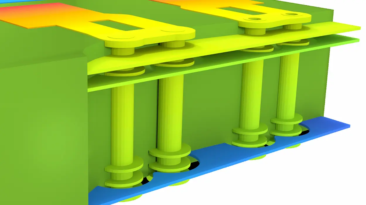
Optimize your Via selection
To optimize your board, you need to choose appropriate via types. Such as blind, buried and through-hole vias, etc. So it is very helpful to control the complexity of the circuit board. Moreover, via selection can also impact your PCB board thickness.
Optimize your material selection
You must choose the best materials on a layer by layer basis. Signal layers in PCB layers stack up must be symmetric and support good signal integrity.
Optimize the manufacture of your boards
The most important point is to choose the best manufacturer for your circuit boards, such as MOKO Technology. Everything matters in layer optimizations such as solder masking, drill hole sizes, and trace parameters. So you should go for an expert team of manufacturers. And MOKO Technology is the best option!