- You can get a soldermask-like material in a small touch-up bottle.
- Maybe you cancut the pad with a razor just to make some space.
- Getting bridging during the reflow process.
Read More: PCB Design and Layout
#PCB Design
Read More: PCB Design and Layout
#PCB Design
To my understanding, each process in the operating system contains its own separate Process Control Block. Can someone explain this to me. Does each process have its own PCB or is there just one PCB that contains all the information for all the processes?
On a Flex Printed Circuit (FPC) made out of Kapton polyimide, will anything bad happen if I put a VIA in a part of the FPC that has to bend? VIA size: 0.2 mm hole diameter in 0.4 mm copper diameter. FPC bend radius: 0.7 mm. Kapton thickness: 0.2 mm. Copper weight: either 2 oz or 1 oz (I haven’t decided yet)
I did have one board come back with a manufacturer error – an extra bit of copper just a hair’s width across hidden underneath a component. It looked almost like someone’s eyelash had fallen onto the board just before photo etch. How should I deal with it?
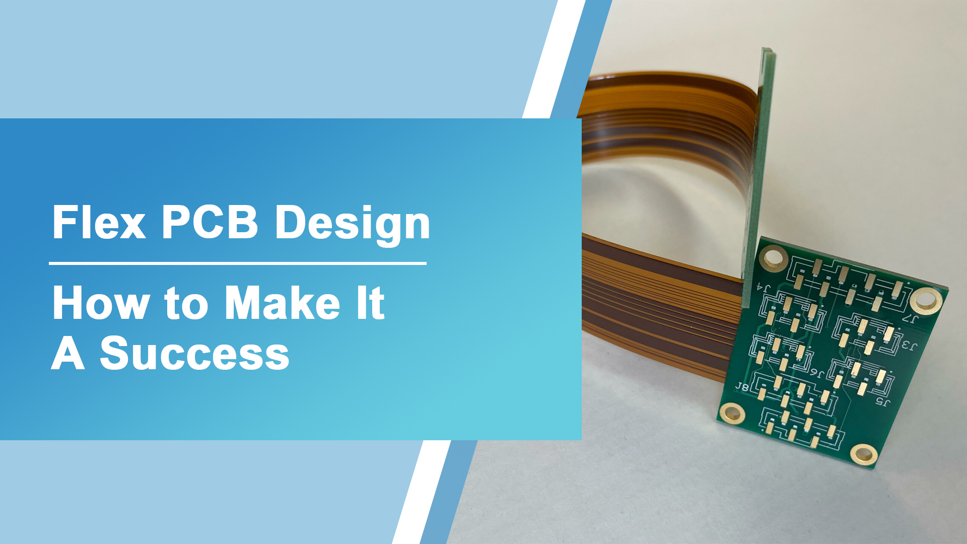
Flex PCBs, or Flexible Printed Circuit Boards, have gained significant popularity in recent years due to their unique properties and advantages in various applications. These
People expect electronic products to be rich in functions, but also require them to be small and portable, which brings new challenges to circuit board
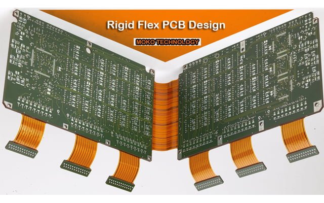
Rigid Flex PCB Design: Benefits and Design Best Practices With the use of a rigid flex PCB(rigid FPC), flexible circuit substrates and rigid circuit substrates
Electronic Manufacturing
Resources
Contact Us
Copyright ©2024 MOKO Technology | Your Trusted EMS Partner 粤ICP备15085690号