PWB and PCB are two terms usually used interchangeably in the electronics manufacturing industry. PWB is an abbreviation for Printed Wiring Board; PCB is an abbreviation for Printed Circuit Board. Although they have similar names, they actually refer to different components.
In this guide, we will explain the precise distinctions between PWB and PCB, as well as the relationship between these two terms, so you can have a clear understanding of each.
PCB VS PWB: Key Differences at a Glance
First, let’s take a quick look at the primary differences between PWB and PCB:
| Characteristic | PWB | PCB |
| Definition Focus | Electrical interconnections (wiring) | Complete circuit platform (performance + structure) |
| Terminology Usage | Legacy / formal term | Modern industry standard |
| Era of Use | Common in 1960s–1980s | Standard from 1980s to present |
| Technical Scope | Emphasizes connections between components | Includes signal integrity, thermal, and mechanical design |
| Modern Relevance | Rarely used today | Widely used across all applications |
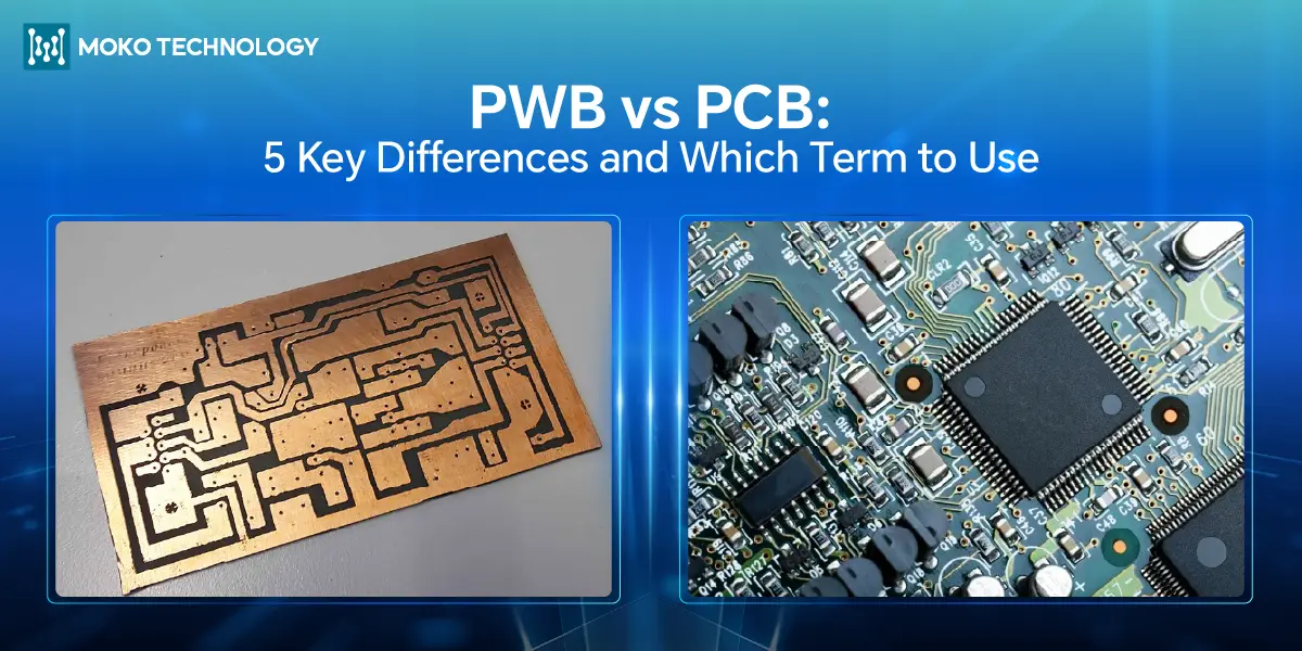
What Is a PWB?
PWB, or Printed Wiring Board, is a board that provides mechanical support and electrical interconnections for assembling and connecting electronic components. This term originated in the early stages of the electronics industry.
At that time, electronic devices were assembled using manual point-to-point wiring, which was not only inefficient but also unreliable. In addition, this method made large-scale production difficult. The introduction of PWB helped solve these problems by providing printed conductive paths on an insulating substrate, replacing “rat’s nest”-like wiring with a neat and structured layout.
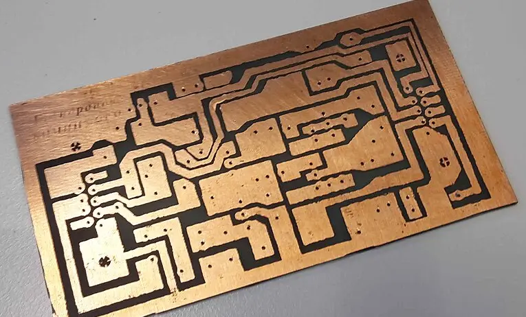
Early PWBs were usually constructed using simple insulating materials such as phenolic paper (FR1/FR2) or early fiberglass. The process used to print or laminate the surface with conductive pathways was comparatively simple – there was no multi-layered lamination, no chemical etching, no finely drilled holes. Therefore, PWBs are quick and cheap to manufacture, but the downside is their restricted capacity to accommodate complicated and high-density circuits.
What Is a PCB?
A PCB, or Printed Circuit Board, is a board made from a non-conductive material on which electronic components are mounted and interconnected using conductive pathways or traces etched onto the board’s surface. PCB provides the substrate on which various electronic components such as integrated circuits, transistors, resistors, capacitors, and other parts can be mounted and interconnected.
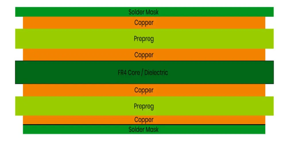
Modern PCBs are built from multiple laminated layers. A typical PCB stackup includes:
Copper foil layers — the conductive pathways (traces) that carry electrical signals
FR4 dielectric substrate — a fiberglass-reinforced epoxy laminate that insulates the copper layers from each other
Prepreg — a bonding layer between copper and core layers
Solder mask — the green (or other colored) coating that protects copper traces and prevents short circuits
Silkscreen — the top printed layer used for component labels and reference designators
5 Primary Difference between PWB and PCB
1. Construction and Layout
The construction methods of PWB and PCB lay the groundwork for their distinctions. PWB typically involves printed conductive paths on a substrate, focusing primarily on wiring. PCB, on the other hand, boasts a more elaborate design, incorporating layers of conductive material separated by insulating layers, facilitating a more intricate circuitry layout.
2. Manufacturing Process
PWB production involves relatively simple steps: applying conductive traces onto a substrate with minimal processing.
PCB manufacturing, by contrast, requires multiple precision steps:
- Step 1: Inner layer imaging — circuit patterns are transferred onto copper-clad laminate using photolithography
- Step 2: Etching — unwanted copper is chemically removed, leaving only the designed traces
- Step 3: Layup and lamination — multiple layers are aligned and bonded under heat and pressure
- Step 4: Drilling — holes (vias) are drilled to create electrical connections between layers
- Step 5: Plating — drilled holes are copper-plated to ensure conductivity across layers
- Step 6: Solder mask and silkscreen application — the final protective and labeling coatings are applied
This level of process complexity is why PCBs can support dense, high-speed circuits that PWBs simply cannot.
Interested in more details on the PCB manufacturing process? Read this blog: A Detailed Guide to the PCB Manufacturing Process
3. Components and Integration
While PWB focuses on wiring, PCB harmonizes wiring and components. Electronic elements are soldered onto the board, forming a symbiotic relationship that enables circuits to fulfill their designated tasks. Printed wiring boards usually lack the integration prowess that PCB offer, limiting their capabilities in complex electronics.
4. Applications and Industries
Printed wiring boards are well-suited for industries where basic electrical connectivity is the primary goal, such as in simple consumer electronics. On the other hand, printed circuit boards, with their capacity to incorporate complex components, are favored where advanced performance is required, such as in computing, automotive, and telecommunications.
To put this in concrete terms:
Take the transistor radio of the 1960s — a device that ran on a single-layer PWB with a handful of components and basic point-to-point connections. Compare that to a modern smartphone motherboard: a 10-layer or more HDI PCB with trace widths as fine as 0.075mm, integrating thousands of components in a space smaller than your palm.
5. Functionality and Complexity
The most glaring distinction between PWB and PCB is the realm of functionality and complexity they encompass. Printed wiring boards serve the straightforward purpose of creating electrical connections between points in a circuit. Their focus is providing the fundamental wiring backbone to link components together. In contrast, printed circuit boards go well beyond just connecting components. PCB integrates a variety of electronic components to build complex, multifaceted circuits and systems.
From a signal integrity perspective, modern PCB design must account for factors that PWBs never had to consider — impedance control, differential pair routing, via stub management, and thermal relief design. These requirements are why PCB design today is a specialized engineering discipline, governed by standards such as IPC-2221 (Generic Standard on Printed Board Design) and IPC-A-600 (Acceptability of Printed Boards).
Why the Industry Shifted from PWB to PCB?
Nowadays, most people use the term PCB instead of PWB. But what is the reason behind such a transition? Actually, such a shift is an indication of the growth of the electronics industry.
PWB was widely used in the period when the electronics industry was still emerging, from the 1960s to the 1980s. The board was mainly used as a mechanical support at that time, with simple electrical connections. Electronic devices had functions that were rather primitive. Then, with the fast advancement of technologies, the board also developed to execute more and more functions in order to satisfy constantly changing demands. At that time, the simple wiring structure could not meet the needs anymore. In this way, the industry slowly came to use the name PCB, which has a more appropriate meaning for the board as a complete circuit platform. However, there is an exception. In Japan, PWB is still sometimes preferred over PCB to prevent confusion with polychlorinated biphenyls, a class of toxic chemical compounds.
PWB, PCB, and Other Related Terms
The terminology surrounding printed circuit boards can be confusing, especially since some of the terms have similar acronyms and can be used interchangeably. In addition to PWB and PCB, there are also other related terms that are commonly used in the electronics industry:
- PCBA stands for Printed Circuit Board Assembly. It refers to a PCB with components mounted on it, capable of performing its intended function.
- PWA, or Printed Wire Assembly, is actually the same thing as PCBA; it is just an obsolete term for PCBA.
- CCA, with the full name of Circuit Card Assembly, it is technically the same as a PCBA. But nowadays, fewer people use this term.
- PCA means Printed Circuit Assembly, it is an uncommon alternate term for a PCBA.
In above terms, PCB and PCBA are the standard terms used today, while the others are mostly legacy terms that appear in specific industries or older documentation.
FAQs about PCB and PWB
What is PWB in electronics?
In the electronics industry, PWB stands for Printed Wiring Board. It is a board with copper traces used for electrical interconnections. However, this is an older term mainly used in the 1960s–1980s. Today, people are more likely to use the term PCB.
Is PWB same as PCB?
PWB and PCB refer to essentially the same type of board. PWB is an older term focused on wiring, while PCB is the modern, widely used term.
What’s the difference between PWA and PCB?
PWA stands for Printed Wiring Assembly, which refers to a board with components assembled on it. In modern electronics, people usually use the term PCBA (Printed Circuit Board Assembly) instead. On the other hand, PCB refers to the bare board that has no components on it.
Is there a significant difference between PWBs and PCBs in terms of manufacturing?
Yes. When manufacturing PWB, a simplified printing method is used where the conductive wires are simply printed on the substrate. Conversely, PCBs go through several processes that include etching, drilling, and laminating multiple layers of conductive and insulating materials.
Conclusion
Printed wiring boards and printed circuit boards represent two pivotal innovations that fueled the electronics revolution. In the early days, printed wiring boards provided a basic platform to connect electronic components with simple wired links. This allowed the first primitive electronic devices to be assembled. However, the real game-changer was the printed circuit board. By etching conductive copper tracks directly onto an insulating board, PCB enabled the integration of many more intricate connections between components in a small space. This density and complexity enabled PCB to support advanced circuit designs packed with components like transistors and integrated circuits. PCB truly catapulted electronics forward from simple circuits to the sophisticated devices that underpin modern tech. Looking back, we can see how printed wiring boards laid the initial foundations, but it was printed circuit boards that really sent electronics skyrocketing into the future. Each technology marked a key milestone along the road of progress.