Different methods of PCB panelization
As with many processes in the electronics industry, there are countless possibilities and variants in the PCB panelization. Since each manufacturer has its own approach, you as a designer have to choose from time to time to adapt your design accordingly or to look for a different partner for production. The three most common methods are explained below:
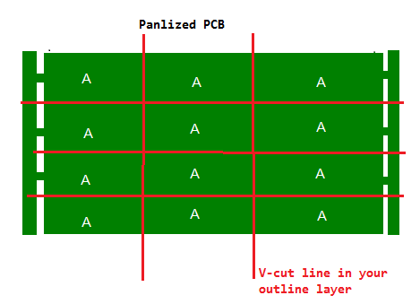
Panelization using V-grooves: With this approach, the individual circuit boards are separated from one another by V-shaped milled grooves with a depth of one-third of the panel height. The later separation is then carried out by a machine that is best suited for straight cuts. This method is therefore particularly recommended for PCBs that meet three requirements: no overhanging components, no rounded corners and a sufficient distance between the component limit and the edge of the PCB.
Panelization through tab routing: Here, the circuit boards are milled out along their contours – while maintaining a handful of material bridges that hold the board securely in place during the manufacture and assembly of the panel. This type of panelization is not suitable for printed circuit boards with large transformers and other heavier components that greatly complicate the separation. At the same time, it should be noted that this method reduces the loads on the printed circuit boards and thus reduces the risk of chipping.
Panelization through tab routing with perforated material bridges: This process is similar to the simple tab routing just described. However, here the material bridges are additionally perforated with small drill holes, which greatly simplifies the separation and also offers a higher degree of control since the course of the fracture is easier to predict. However, this method is even less suitable for printed circuit boards with heavy components, the weight of which can break the material bridges.
The disadvantages of PCB panelization
Paneling PCBs is one way to protect its integrity. In addition, panelization enables China PCB manufacturers to assemble multiple boards at the same time, reducing costs and production time. The paneling must be carried out properly so that the printed circuit boards are not damaged or otherwise damaged during the separation.
Challenges:
Paneling presents a number of challenges in several areas:
1.Depanelization- disadvantages of some depanelization methods:
If using a router, additional cleaning may be required before shipping. This method creates a lot of dust that has to be extracted.
2.Replacement of parts pre-routing required to avoid interference with depanelization:
Protruding components can fall into adjacent parts.
3. Incomplete data files – sometimes incomplete files are provided by PCB manufacturers, which can increase costs in several ways:
“Breakaway holes” or “mouse bites” – These tiny holes allow the use of small circuit boards in an array.
Cumulative and Registration Tolerances – If there are no tight tolerances in the data file, the cumulative effect of tiny deviations can lead to errors. If there are several boards in the array, the registration can no longer be centered.
DFM and PCB panelization
When companies develop printed circuit boards for large quantities, they look for ways to reduce manufacturing costs with little tricks and tricks. This requires only relatively little effort if the details of the production are discussed in detail in the early phase of the design process and taken into account in the development of the printed circuit board (which is therefore highly recommended). This early optimization of the layout with regard to the planned manufacturing processes is generally referred to as “production-oriented design” or “Design for Manufacturing” (short: DFM).
There are various DFM methods with which considerable savings can be realized in the long term. My preferred strategy is simply to get in touch with the manufacturing companies early on and to find out about their specific skills, challenges, and business models. In this way I can get an idea of which aspects of my design can be implemented easily (and therefore inexpensively) and which elements are associated with additional effort (and correspondingly higher costs).
I benefited from this a few years ago, for example, when I designed an amplifier for a loudspeaker and initially favored a PCB with a round form factor since it could be mounted directly behind the likewise round chassis of the loudspeaker in a visually appealing way. However, when I discussed my idea with the manufacturer, it quickly became apparent that PCBs with a (supposedly simple) round shape is so expensive to manufacture that this greatly reduces the economic viability of the design.
So, in the end, I decided on a rectangular standard design, the manufacturing costs of which were considerably lower. By adjusting my layout accordingly, I was able to increase the profit margin of the end product and bring the project to a successful conclusion.
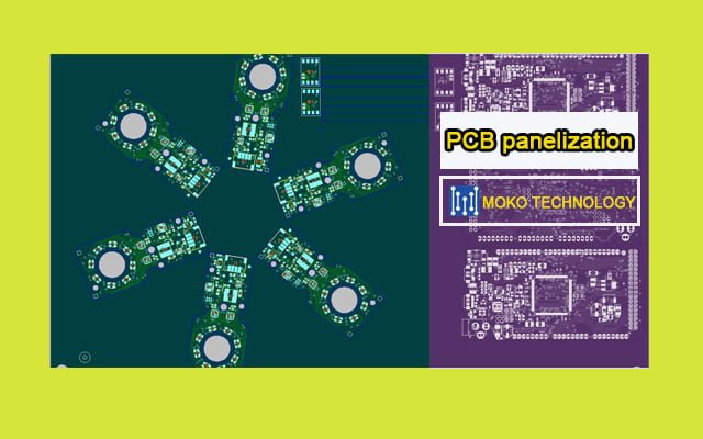
PCB Paneling cuts costs
A low widely used DFM approach is the so-called panelization. With this method, several circuit board layouts are applied to a larger substrate or panel and then assembled in this form. The desired savings result from the possibility of manufacturing several PCBs at the same time.
After the manufacturing and assembly process has been completed, the panel is then divided into the individually printed circuit boards. This way you get a whole bunch of finished and (hopefully) fully functional PCBs in one fell swoop, just waiting to be installed and sold. That sounds pretty easy, doesn’t it? But not so quickly: So that the PCB mass production later runs as smoothly as possible and brings the desired savings, some important subtleties have to be taken into account when paneling.
Factors that affect PCB panelization Cost
Of course, most designers are ultimately less interested in the technical details of the various processes than in the associated costs and challenges. The basic rule of thumb here is that costs and effort depend on the complexity of the design to be manufactured and grow with it. It should also be noted that panelization-based manufacturing poses the following challenges, which also have an impact on costs:
Separation: If a milling machine is used to separate the fully assembled printed circuit boards, chips, and other residues remain on the surface of the PCBs, which must then be removed at a later point in time in a separate step, which involves additional effort and costs. If you want to use a saw instead of a router, you should take into account when designing the contour of your circuit board that only straight cuts are possible here. A third option is to use a modern laser, which, however, can only be used for PCB thicknesses of 1 mm or less, so that in this case you cannot create multilayer PCB designs of any thickness.
Fractures: Most separation processes leave rough fractures on the sides of the workpieces – especially in the case of panelization through tab routing with perforated material bridges (see above). So that the individual PCBs can be handled safely, they have to be ground down at the points in question, which in turn means additional work.
Overhanging components: As already mentioned, overhanging components can drastically limit the number of panelization methods that can be used for your design. In such a case, there may also be problems with the separation of the finished PCBs, since there is a risk that the milling head will collide with an overhanging component and thereby damage the entire panel. It goes without saying that such breakdowns involve unforeseen costs and delays.
PCB Supply Chain: A complete and stable PCB supply chain helps manufacturers to obtain sufficient components and other raw materials at competitive prices, while any component shortages will not only slow down manufacturing progress, but also increase your PCB panelization cost.
Possibilities for early detection and preventive remedy of potential problems
Experienced PCB designers rely on various proven methods for the early detection and correction of potential problems.
As already mentioned, a design based on DFM principles can effectively ensure that paneling and production are as cost-effective as possible. For PCB panelization, it is necessary, among other things, to find out about the right manufacturing companies and their manufacturing processes in the early phase of the design project. This way you can optimally design your layout for production right from the start.
In addition, many challenges around automated PCB manufacturing are easier to master if you use first-class design software. For example, Altium Designer® offers extensive functions for PCB panelization via the “Embedded Board Array” feature. This allows you to easily assemble a panel with several identical or different PCB designs. And since the original designs are not simply copied into the panel, but linked to it, changes to an original design are immediately apparent in the layout of the panel.
Of course, there are many other ways to save manufacturing costs in addition to the paneling. Nevertheless, this point deserves special attention, since errors here quickly result in unforeseen additional costs or even completely unsuitable PCBs.
Therefore, you should definitely heed the advice and DFM principles found here – and in numerous other articles – and pay attention to production-oriented design throughout the entire design process. This not only saves you time but can also reduce manufacturing costs and the risk of subsequent corrections.
If you’d like to learn more about how Altium can help you overcome your paneling challenges, speak to one of our experts today.
EXTENDED GERBER RS274-X – PCB data
– If your design system allows it, use the extended device RS 274-X for data export. The main advantage is that all information about the shape and size of the panels is contained in the header. Data import is easier and it minimizes the risk of incorrect preparation of the panels. The data processing time is also significantly reduced, which also affects the lower costs for data preparation.