The circuit board is the heart of electronics and computing devices. This circuitry transmits signals from control prompts to the screen. For example, you can find a circuit board in your smartphone. When you touch the screen, you activate one of the signals on this circuit board every time. PCB vias are essential for enabling the complex circuitry required for modern devices to function. Among the various types of vias, microvia is particularly important.
What Is a Microvia?
Micro vias are the remarkable component of high-density interconnect boards. These are a special type of vias having a size 150 micrometers or less. Due to their small size, designers prefer micro vias and use them in HDI boards. The microvia needs far less space as compared to other vias on the board. In a micro via, copper plating connects different layers of the board with each other.
Types of Microvias in Printed Circuit Boards
There are four commonly used microvia types including blind micro vias, buried microvias, stacked microvias, and staggered microvias. You can use individually or combined to increase the density of printed circuit boards.
Blind microvia
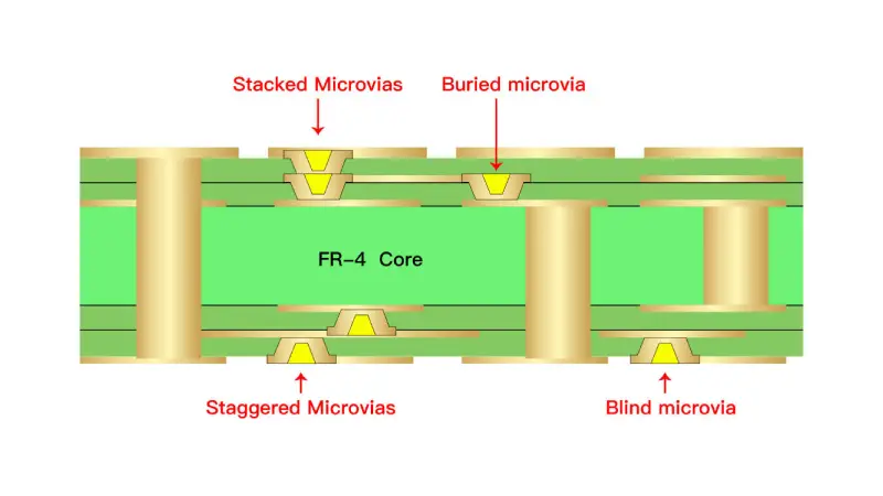
If a microvia starts from the outer layer and stops at an inner layer known as blind micro via. It means it doesn’t penetrate both layers. By using blind micro via, you can enhance the density of wires on the circuit boards.
If you want to route a signal from the outer layer to an inner layer, blind vias are very useful. They provide the shortest distance in this scenario. On the HDI board, these micro vias are used to optimize the space of multilayer boards. For example, if a board has four layers, you can place these vias either on the top two or the bottom two layers.
Buried microvia
A micro via that connects two internal layers of the board is known as a buried micro via. These vias are not visible from the outer layer. So if you want to include buried via your circuit board. Then you will have to drill the inner layer before applying the outer layer. You can connect two inner layers by using buried via. You can use any mechanical tool for drilling. However, the best alternative method is to use a laser for this purpose.
You must pay attention to the aspect ratio of the hole size before applying micro via a circuit board.
Further reading: Blind Via & Buried Via: What’s the Difference?
Stacked Microvias
Stacked microvias enable vertical electrical connections across multiple PCB layers. A hole is drilled through one layer, then another aligned hole into the next layer below. The holes are metallized, creating a conductive path between layers. This stacking approach allows high-density routing. Stacked microvias are crucial for HDI PCBs found in high-performance computing, communications systems, and IC packaging applications requiring immense circuit density in limited space.
Staggered Microvias
Staggered microvias are a method in high-density interconnect (HDI) printed circuit board (PCB) design where microvias (tiny drilled holes for electrical connections between layers) are not directly aligned on top of each other but are offset. This arrangement connects alternating layers and is used to enhance board reliability by reducing stress and potential for damage. Staggered microvias facilitate complex routing in multi-layer PCBs, allowing for denser circuit designs without compromising the structural integrity or functionality of the board, crucial for advanced electronic devices.
Further reading: Stacked Via VS. Staggered Via: What’s the Difference?
What Are Microvias Used For?
Look at the trends of current electronic and computing industries. Both industries are looking for lighter, smaller and more reliable electronic devices. It means industries are considering these appearance factors besides functionalities. Moreover, performance is the crucial factor to put a device in trending.
To make a device lighter and smaller means you need to create circuit boards smaller and lighter. If circuit boards are giant, it is impossible to create a smart device. Moreover, if the circuitry is giant, it will consume more energy. So battery timing will be low again. All industries want to consume batteries as low as possible. So small circuits will be handy in this situation.
In addition to this, small circuits produce less heat. So again battery consumption will be low here. Moreover, these small circuits have excellent performance. Your smartphone performance is the witness! To increase the functionality of a circuit, you need a complex routing mechanism. Smaller circuit boards came into existence such as Ball Grid Arrays due to the higher numbers of input and output. It means when I/Os increase, you need to increase the circuit traces on the same boards.
To tackle such problems, researchers came up with various solutions. One of the solutions was to use high density interconnect technology with micro vias. By using many vias, the circuit board can carry more traces. More traces means a denser placement of different components. The main purpose of microvia is to increase the density of the circuit board. Micro vias and HDI technology combined make it possible to carry six components in a specific area. Prior, to this area, conventional methods just carried four components.
Why Is Microvia Better Than Other Types of Vias?
The PCB manufacturing process is an expensive process. This process becomes far more costly when you need to create complex circuitry. So it is a fact that each layer in the circuit boards costs a lot. Therefore, when layers increase, the cost of the circuit board will increase.
So you can utilize microvia to replace the conventional through-hole vias. Through-hole is a very common terminology. It means normally when we talk about vias, we are considering through-hole vias.
What would happen if you replace through-hole vias with micro vias? It will decrease the number of layers which means reducing the manufacturing costs.
Besides this, a minor replacement can’t only cut decrease the cost. But also enhance the electrical characteristics of the PCB. In the age of technology, people go with the smaller and lighter devices. Therefore, high density and multilayer circuit boards are the need of this era.
Besides functionalities, microvia utilizes the minimum space of the board. Furthermore, they come in just two are three layers. So the manufacturer gives priority to these vias.
In addition to this, micro vias are available in a wide variety of patterns and materials. It makes this technology one of the finest choices of complex circuit boards. Such as staggered, via in pad and non-conductive are some of the examples. It further includes staked, offset and copper-filled material.
You can boost routing across multiple layers by using stacked micro vias in those applications requiring more than three layers. Furthermore, it also gives a built-in thermal regulation.
Wrapping Up
Microvia usage is essential as electronics shrink and densities increase. Proper design and manufacturing of these tiny interconnect vias is critical for PCB performance and reliability. If you lack in-house know-how, consulting specialists could prove invaluable. MOKO Technology offers integrated PCB design and manufacturing services. We guide customers through microvia implementation to optimize high-density interconnects. Feel free to contact us to get a free quote.