Do you remember IBM Simon? You can consider it the father of smartphones. The Simon phone has 38 mm thickness and almost 510g weight. So it was impossible to place in the pocket. On the other hand, look at today’s smartphone. You can easily put them in your pocket. And the reduction in the size of a smartphone is due to the HDI PCB. The purpose of HDI technology is to make devices smaller, thinner, and lighter as well.
So do you want to learn HDI PCB? This article gives you a clear idea about what is HDI circuit boards. So we will cover its features, benefits, and applications, etc. After reading this article, you will be adept in HDI PCBs.
What is HDI PCB
HDI PCB stands for High Density Interconnect Printed Circuit Board. It is one of the significant enhancement in the world of electronics. Moreover, its advanced multiple via processes minimizes the number of layers. So it provides smaller yet most powerful circuitry.
Features of HDI PCB
HDI PCB fabrication uses the latest multilayer technology that allows you to integrate multiple layers with high density. This technology has significant dominance over other traditional PCBs. Here are some key features of this technology:
- High-density interconnector uses laser drilling technology. So this technology precludes different drawbacks that occurred during traditional mechanical drilling technology. Therefore, it reduces your difficulties.
- These boards contain high wiring density per unit surface area as compared to regular PCBs.
- HDI boards most often come with apertures having a range of 3.0 to 6.0 mil. Moreover, the line width is between 3.0 and 4.0 mil. So by using these features, you can minimize the pad size significantly.
- Another most popular feature of these boards is vias. There are different types of PCB vias such as buried, blind and micro vias. The size of the vias can be lesser than 0.0006 mm in diameter. So these small size vias help you to save more space on the boards. So you can create a more compact design.
- The effectiveness of these boards assists as a substitute to use of high-layer laminated boards. Moreover, these boards are expensive as well.
- Different characteristics such as lightweight and high frequency. Plus, high electrical speed makes it the ideal option for various applications.
Different Types of HDI PCB Stackup
According to the IPC-2315 standard from the IPC, there are 6 basic types of stack-ups. These stack-ups types include I, II, III, IV, V and VI. However, the last three types are more expensive and have minimum use. So we will only discuss the first three types of vias. Moreover, the standard differentiates HDI stack-ups on the basis of the vias type. Such as micro, buried, blind and plated through vias.
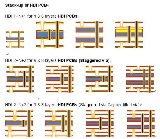
- HDI Type I: These types have a structure of a laminated core having at least just a single layer of micro vias. These vias can exist on one or both sides of the circuit. Type I HDI use blind and PTH vias. However, it doesn’t use buried vias.
- HDI Type II: This type includes different blind and buried vias on a laminated core. Fabricators can stagger different micro vias and stack them relative to buried vias.
- HDI Type III: To construct this type, the manufacturer uses micro vias, buried and blind vias on a laminated core. Moreover, this type includes at least two layers of micro vias on one side of the board or both. You can stagger micro vias over other micro vias. Furthermore, you can stack them over other buried vias.
HDI PCB VS Standard PCB: Key Differences

Due to their use of small blind and buried vias, HDI printed circuit boards offer superior signal integrity over standard PCBs by minimizing stray capacitances and inductances. Microvias in HDI PCBs lack stubs, so their impedance closely matches that of the trace. In contrast, the higher stray capacitance of vias in standard PCBs creates larger impedance discontinuities.
Some key differences between HDI board and conventional PCB:
| Feature | HDI PCB | Standard PCB |
| Component Density | Higher | Less |
| PCB Size | Smaller and lighter | Larger and Heavier |
| Via Type | Blind, buried, and microvias | Through holes |
| Number of Layers | Lower | Higher |
| Compatibility | Compatible with high pin count and low pitch packages | May face compatibility issues with low pitch packages |
Benefits of Using HDI Board
Using HDI circuit boards in your application has a lot of advantages. Due to these benefits, most manufacturers prefer HDI over other types of circuit boards. Have a look at the benefits of using HDI PCB in your applications:
Reduce heat transferring
Traditional PCBs burn due to a lack of heat transferring. So this technology has an edge over traditional circuitry such that it reduces heat transfer. Why? It is because the heat has to travel for a short distance before leaving the HDI PCB.
The design of this circuity makes it capable to go through a high thermal expansion. So it increases the lifespan of the circuit boards.
Manage thermal conductivity
The availability of different types of vias makes sure the current transmission between the components. So it is up to you to fill these vias with either conductive or non-conductive materials. You can further enhance the functionalities by using the blind vias and via in-pad components together.
Furthermore, the HDI boards have a compact structure. So it reduces the transmission distance between different components. It further reduces transmission times and crossing delays as well. So as a result, you will have a strong signal for your circuit.
Minimal power usage
HDI PCBs consume less battery power as compared to traditional ones. This is because of advanced manufacturing technology. This technology binds the electrical components resulting in minimizes loss of energy.
HDI circuits use vias instead of through holes that also reduce power usage. This effect increases the lifespan of your battery.
Smaller form factors
It is an ideal choice for saving space. You can easily minimize the total number of layers on HDI PCB designing. For example, you can replace the 8-layer through holes by using a 4-layer via in pad solution. As a result, you will have a small PCB. Some vias will not visible to the people and increase performance as well.
Incorporation of components
You can’t only minimize the space but also incorporate your boards as well. It means you can put as many details as you want on the HDI board. Furthermore, you can populate both sides of the board to incorporate the components. So this depends on the design and the need for the application.
Different designs
By using the high-density interconnector technology, you can create different designs of the boards. So you can use these circuit boards in all applications as you want. Such as you can have rigid, flexible and combination of both.
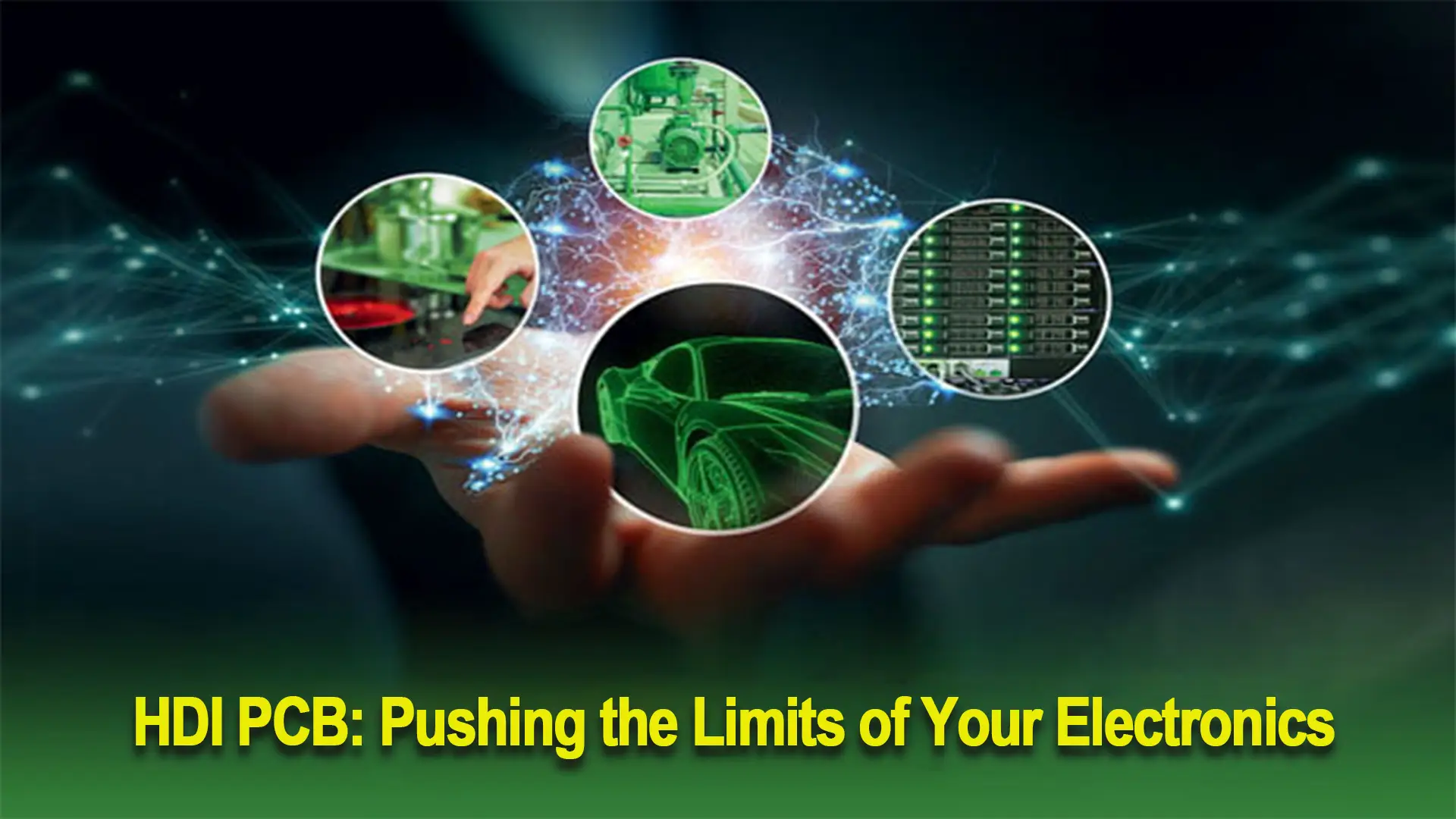
Application of HDI PCBs
So far you have learned a lot of things about this amazing technology. However, you might be thinking that where you can apply these incredible circuit boards. So it is a fact that there are countless applications where you can use this board. Therefore, you can use this circuitry from simple to mega-complex applications. Here are some significant applications for HDI PCBs:
Consumer electronics
This term refers to all basic devices you find in your daily life usage. Such as laptops, smartphones, and cameras. Moreover, it also includes the majority of home appliances and entertainment systems.
All these gadgets need circuit boards having lighter weight. Moreover, these appliances also need flexibility. Thus, HDI circuitry meets the qualities of these gadgets.
Medical equipment
There are numerous electronics playing a key role in the wellbeing of our health. So the medical industry wants to ensure the high-quality circuits that meet their standards. So all medical equipment should be effective and play a major role in the safety of the patient.
So there are several devices where you will find HDI printed circuit boards. Such as monitors and scanners. It further includes heart pacemakers, scientific instruments and control systems.
Industrial applications
You can find this circuitry in high-powered industrial applications. Due to its effectiveness and robust nature. Moreover, it consumes less energy and ensures maximum output.
Even these circuit boards are capable to perform in a harsh environment. So most boards use thick copper that helps in faster battery charging. Moreover, it also helps in high current applications as well.
So you can find this circuitry in various applications. Such as electric drills and different measuring equipment. Besides this, they exist in power equipment such as generators and solar power panels.
Automotive
Most automotive rely on different electronic parts to work properly. So you can use this technology in these applications. You can use high-frequency signals of RF and HDI PCBs combined with sensor applications. This is common in automotive.
Different technologies such as radar technology are clearing their way in the automobile industry. All such technologies rely on HDI circuitry.
In addition to this, some common applications such as engine management systems use this technology. It further includes navigation devices, video, and audio devices.
Aerospace applications
The precision and durability make HDI an ideal choice for aerospace applications. Moreover, HDI circuits can resist vibration effects. Airplane and jets need circuity that can withstand in harsh environments.
So HDI circuit boards ensure the security of aerospace applications. These apps include monitoring equipment such as pressure sensors. Plus, accelerometer.
Suggestions for Optimizing HDI PCB Design
- When designing an HDI board, carefully consider the via types you use. Micro vias, blind vias, and buried vias can reduce layers and costs. But through-hole, dog bone, and via-in-pad vias make manufacturing more complex. Choose what works best for your design needs and budget.
- Also be selective with components. HDI requires fewer components with tight spacing. While performance matters most, check packaging, availability, and lead times too. Swapping parts late in the game slows things down and drives up costs.
- Mindfully place components to minimize uneven stress and EMI. Too many vias clustered together can warp boards and ruin yields. And dense spacing risks crosstalk or signal noise from parasitic capacitance and inductance. Do modeling early to catch these issues.
- Take time to optimize routing. HDI traces can be narrower, but make sure widths suit signal performance. Keep lengths short, impedances consistent, and provide ground planes. Isolate digital, analog, and power to prevent interference.
- Finally, balance material stacks and layers with affordability. More layers or exotic materials increase lamination and drilling expenses. Weigh the benefits against your budget constraints.
To find out more details about HDI PCB design, check out our other blog: https://www.mokotechnology.com/hdi-pcb-design-guidelines/
Working with The Trusted HDI PCB Manufacturer
When it comes to advanced PCBs, high-density interconnect (HDI) boards are in a league of their own. HDI technology is robust and versatile, able to serve countless applications. So if you need reliable HDI PCB manufacturing, MOKO Technology is a great choice.
Our skilled engineers have deep expertise in HDI designs and our manufacturing facilities are state-of-the-art. This winning combination enables us to produce sophisticated, high-performance HDI printed circuit boards to meet your exact specifications. Click the picture below to get in touch with us!