Have you ever opened up the case of a broken smartphone or smartwatch? If yes, you will be familiar with small circuits packed into such small devices. Different electronic components are shrinking day by day. However, the performance of these devices is dramatically increasing. This change has occurred due to the microvia PCB.
In this informative article, you will learn about microvia PCB design and cost consideration. Furthermore, we will explain its challenge. Let’s have a look at what are microvia PCBs and why they are cost-effective.
What are the microvia PCB ?
All PCBs contain stacked pads that have small holes. These holes have some sort of electrical connection with each other for the flowing of the current. These conductive holes are vias.
Certain products, especially those used in computing industries and telecommunications need a special type of PCB with vias. Such PCBs contain a great number of highly dense layers with very small vias to enhance functionality.
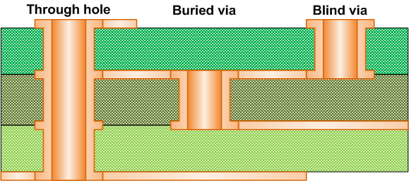
Microvia PCB has three major parts:
- Through holes: These micro vias penetrate all layers of the circuit board.
- Buried vias: Such microvia exists in the middle layers of boards. Moreover, they don’t have any exit to the exterior.
- Blind vias: These micro vias don’t penetrate the entire circuit board. However, they connect the exterior layer to at least one layer of the board.
Design consideration of micorvia PCB
Microvia PCB design has the highest wiring and pad density as compared to other conventional PCBs. Moreover, they come with smaller spaces and trace widths.
The size of the microvia PCB is extremely small. So you can use these to create the most compact designs. Besides this, you can use these vias up to a drill hole depth of about 100 micrometers. You need to use a laser drill for microvia PCB. So due to its short barrel, you don’t face any problem with different expansions. So this technology is more reliable as compared to the through-hole vias.
When talking about complex circuit boards, different experts highly recommend micro vias solutions. The dimple occurred due to the microvia raise the risk of voiding somehow. However, you can easily control it with suitable soldering conditions. Moreover, additional microvia filling process can reduce the risk of dimples. In this situation, you will have to pay extra money.
For 0.65-micrometer pitch BGAs, micro vias are very suitable. It may need to reduce the track width of BGA to 90 micrometers. Or even less than this.
Furthermore, the BGA 0.50 micrometer pitch also needs microvia PCB. It can be necessary to decrease the pad size of the micro vias to 75 micrometers.
Cost consideration for microvia PCB
Microvia is very tiny and use to connect high-density layers. According to IPC standards, these vias must be 150 micrometers or less in diameter. Microvia PCBs are very helpful to create the compact circuit board. These boards are very expensive due to several reasons. For example, they contain complex circuitry and compact designs. Moreover, there involves a complex build-up process in fabrication.
However, there are several situations where you can use micro vias to reduce the cost of circuit boards. Here are a few simple scenarios where you can reduce the overall manufacturing cost:
- Reduce layer count to reduce cost
Are you using through-hole vias in your design? Plus if using the trace escape for BGA is not working smoothly. So consider widening the breakout channel on the inner and bottom layers as well with blind vias or micro vias.
- Eliminate electrical layers
Micro vias have the smallest size that is very helpful to maximize the routing channel. If you eliminate the electrical layer by introducing microvia at the place of through-hole vias. You can reduce the cost of printed circuit boards. So by replacing through-hole vias with the micro vias will reduce the layer. If circuit boards have fewer layers, it means those are less costly.
The challenge of microvia PCB fabrication
There are different challenges associated with the fabrication process of micro vias. If you mishandle these challenges, it can lead to ICDs and flaws. The ICD stands for interconnecting defects. These flaws occur near the inner copper layer. The ICDs can cause different problems such as open circuits and reliability problems. Furthermore, you can face intermittent problems at high temperatures that resulting in circuit failure.
It is a challenging process to detect ICDs. Because they work fine during the testing process. You can detect issues during assembly or after using it. So it is very important to fabricate boards carefully to avoid the problem in the future.
Debris-based ICDs
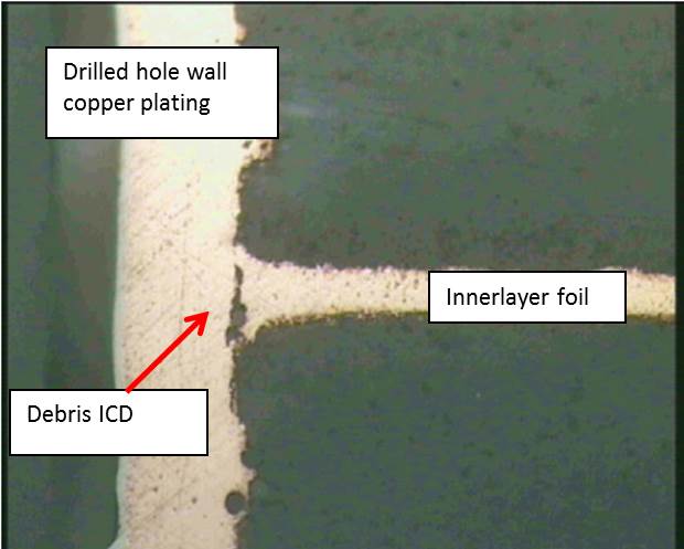
It is one of the common types of ICD. This occurs because debris ends up during the interconnection hole and becomes embedded in the inner-layer copper. This happens most often during the hole-drilling process. Although you drill microvia PCB by using the lasers. And laser doesn’t create holes nearly as much debris as other drilling processes. Therefore, micro vias have fewer chances of ICDs. Still, it is important for manufacturers to be careful.
Voids and reliability
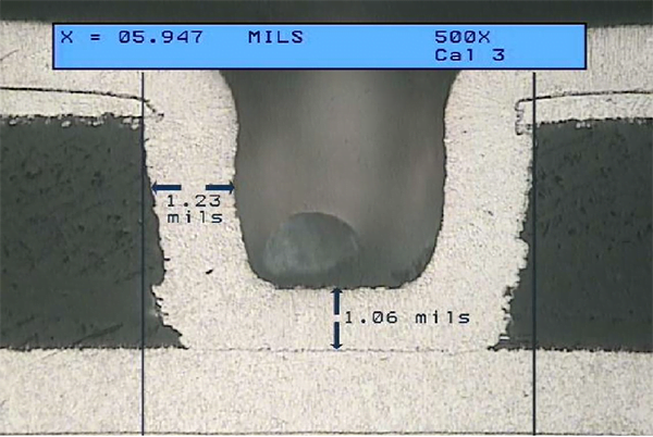
Other problems that occur during the copper plating process for micro vias are dimples, incomplete filling, and voids. These defects or flaws can lead to reliability issues. Incomplete copper filling increases the stress levels in micro vias. Moreover, it decreases their fatigue life.
The impact of voids over micro vias depends on the different characteristics of the void. Such as shape, location, and size. For example, Small and spherical voids can increase the fatigue life of micro vias. Moreover, extreme voiding situations reduce their life.
Copper-bond failure ICDs
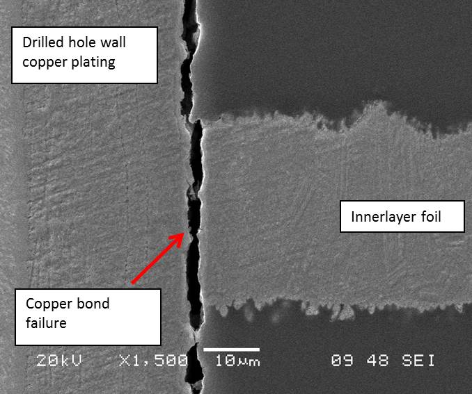
Copper bond failure is another common type of ICD. This can occur due to the high stress during assembly or usage. Furthermore, it can also occur due to the weak bond of copper. When copper bonds fail, interconnect defects occur. In this situation, the copper connection breaks off physically. If the coper bond is weaker, there are high chances of bond breakage.
Why does copper bond fail? There are different reasons. For example, many manufacturers use thicker PCBs and lead-free soldering temperatures. Moreover, the large size of holes and wave soldering can also lead to copper bond failure. Copper bond failure is a common problem in standard vias and microvia PCB manufacturing as well.
Never trust a microvia PCB manufacturer that offers you the cheapest price, trust those who are truly experienced with enough capacities to satisfied you!
We have over 17 years of experienced on PCB manufacturing and PCB assembly, why not visiting MOKO Technology and see if we’re the China PCB manufacturer you’re looking for!

