Single-sided PCB, also known as single layer PCB, is one of the most common types of PCBs. It has conductive material on one side, and another side contains electronic components connected electrically to each other. This detailed article covers different aspects of single-sided PCB. So here you will learn the complete manufacturing process, advantages and disadvantages of this technology. Moreover, we will have a look at the application of a single layer PCB.
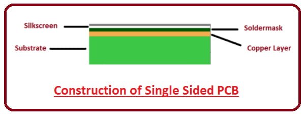
Construction of Single-sided PCB
Single-sided PCB is mainly composed of the following layers:
- Substrate
The substrate layer provides mechanical support for the PCB, it is usually made with insulating materials such as FR-4 (glass-reinforced epoxy), polyimide, CEM, etc.
Further reading: Different Types of PCB Substrate Material for Your Project
- Copper Foil Layer
A thin layer of copper foil is laminated onto one side of the substrate. This copper foil carries the etched circuit traces and connection pads for components. Typical copper weights used are 1 ounce or 2 ounces per square foot.
- Solder Mask
A solder mask coating is applied over the copper, leaving just the required pad areas exposed. The solder mask insulates the traces and prevents accidental solder bridges from forming during component assembly.
A layer of silkscreen polymer ink is printed on the PCB to display text, symbols, logos and other markings. This is useful for component identification, assembly instructions, and branding purposes.
Tips for Designing and Manufacturing Single Layer PCB
Before we move towards single layer PCB manufacturing, there are some important things to consider. With the help of these tips, you can have your boards ready in the minimum time. Moreover, you can save a little amount of money as well. So we don’t further ado and let’s move straightly towards the 8 practical tips:
- Never skimp on quality materials
Never ever ask your manufacturer to choose a cheaper substitute material. If you choose a cheaper one, what if it fails within weeks? You should be familiar with the basic building blocks of PCB. Always go for quality material. These are long-lasting components so it will save you time and money as well.
- Always go with standard board shapes
It is important to choose the standard board shapes. Unless you have a specific-shaped enclosure to fit your design. So always choose a standard rectangular or square shape design. Doing anything out of the norm will cost you more.
- Avoid holes that are too small
If your circuit board contains smaller holes, a higher manufacturing cost. Many fab houses even extra charge if the diameter of the holes is smaller than 0.4 mm. So if you don’t need any specific hole size, you should go with the regular hole size.
- Use the right via
There are three types of vias – Blind, buried and through holes. The blind and buried vias are for high density and high frequency PCBs. So if you don’t need these vias, leave them to avoid the extra cost.
Further reading: Blind Via & Buried Via: What’s the Difference?
- Don’t go for extra layers
Before adding additional layers for more routing space, performance and power plans, think twice. The difference between the two and four-layer board is double! So keep your design clean and compact to avoid paying extra money.
- Setting up design for panelization
You can ask for a giant panel with different other PCBs. You can save a lot of money by choosing the largest panel size. To get your all boards on a single panel, the machine doesn’t need any additional time to set up. As a result, they cost less.
- Go for industry-standard sizes and components
If you have chosen a company for circuit manufacturing, you should choose the standard size of the circuit board. It makes the job easier and more efficient as well. So customizing your order needs extra set up that costs more.
- Choose surface mount components if possible
If you are not building a very complex design, you should stick with standard surface mount components. It reduces the number of holes drilled on your boards. Resulting in lower cost.
The Manufacturing Process of Single Layer PCB
Here is the step by step guide for manufacturing single layer PCB:
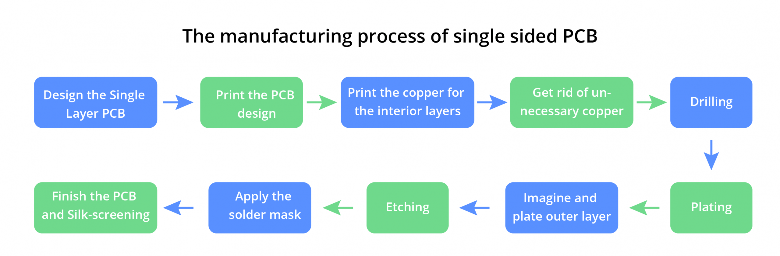
Design the Single Layer PCB
Designing is the first and foremost step to create any circuit board. Moreover, the designing process starts with planning. Designers create a blueprint for the circuitry. In the design, they cover all the requirements of the client.
Print the PCB design
After creating a blueprint of a circuit board, you can now print the PCB design. You can’t print this plan on ordinary architectural drawings. Instead, you need a plotter printer for printing this design. The plotter makes a film on the circuit board.
Furthermore, the printer needs two types of inks, black and clear inks. Black ink for the copper traces and clear ink for non-conductive areas such as fiberglass of the internal layers.
On the other hand, for outer layers, black ink refers to areas where the copper removal process takes place. Plus, clear ink refers to the line of copper pathways.
Print the copper for the interior layers
It is the first step where actual manufacturing starts. After printing lamination, you add a copper layer to it. That serves as a structure for the PCB. You will have to add a photo-sensitive film called resist on the laminate panel. Here you need to perfectly match both blueprint and laminate panel with resist. If both don’t match, try to make it according to the blueprint.
Get rid of unnecessary copper
In this step, you need to remove unwanted copper from the circuit board. You can use a different powerful chemical that can eat away the copper not covered by photo-resist. After removing the copper, now remove the phot-resist from the PCB as well.
Drilling
All PCBs need holes to attach different components and mount the PCB. Before drilling, you can use the X-ray machine to locate the drill spot. There are different ways to drill a hole in the single-layer PCB. However, different systems use solid carbide cutting tools. These tools effectively drill precise holes in the specified locations. Designers provide complete information related to drilling in an NC drill file. So the drill machine works according to the program and drills the required size hole in the exact location.
Plating
After drilling the panel, you can start plating. This process utilizes a chemical to fuse different layers together if exist. After cleaning the circuit board, you need to bathe the board in a series of chemicals. This process coats the panel in a micron-thick layer of copper. Before the holes are filled with copper, the process serves to expose the fiberglass sheet. The fiberglass sheet makes the inside of the panel.
Imagine and plate outer layer
After plating and copper composition, you must apply the outer layer images to prepare the panel for electroplate. There are different types of machines you can use for this purpose such as a laminator machine. So utilize the laminator machine to coat the outer layer using dry film. This dry film is a photo imageable material. Almost this process is similar to the internal layers of PCB.
Etching
When you want to etch the outside layer, you can use the tin guard to protect the copper during the etching process. So in this process, you need to remove the uncovered area of copper. Moreover, traces and pads around the hole and copper pattern will remain there. So you will only remove exposed copper.
At last, you will have to remove the tin as well that is covering the holes and traces. So after completing this step, you will only see exposed laminate and copper of the circuit board. Now you have completed the skeleton of PCB, now onwards you will learn how to protect single layer PCB.
Apply the solder mask
Solder mask protects boards from short-circuiting. Moreover, it also protects the circuit from other environmental effects. So you can use liquid photo imageable solder mask to protect copper surface. In addition to this, it also protects solder bridging between different components in the assembly process.
Finish the PCB and Silk-screening
As part of the finishing process, plate the circuit board with silver, gold or HASL. After final touching the circuit board, you can silkscreen your entire board. In this process, you can print different symbols or information on the circuit boards.
The Advantages and Disadvantages of Single Sided PCB
Single-layer PCB is the simplest circuitry as compared to double-sided and multilayer PCBs. It is very useful for simple electronic components. On the other hand, this circuitry fails when there comes the most complicated electronic device. For example, you can’t use it in the satellite systems.
Here are different pros and cons of single layer PCB:
Pros of single-sided PCB
- As it is very simple, so it is very easy to design this PCB. Moreover, there are almost zero chances to make an incorrect design.
- This is less costly as compared to all other types of PCBs. Cost becomes much lower especially when an order in the bulk quantity.
- As it contains just a single layer, so drilling, soldering, and component inserting process are straightforward and easy.
- Installation of components takes place at only one side, so it needs a lower jumper to compensate for the circuit.
Cons of single-sided PCB
- These circuits are too simplistic for complex projects.
- Single-sided boards have a lower operating capacity.
- Moreover, they are larger in size.And due to their larger size, these have a higher weight.
- With just one side available for placing components, the density of components is limited.
Single-sided PCB vs Double-sided PCB
Single-sided and double-sided PCBs are the two most commonly used PCBs. Below we have included a table comparing their key aspects:
| Feature | Single-Sided PCB | Double-Sided PCB |
| Number of Copper Layers | 1 | 2 |
| Component Placement | 1 side only | Both sides |
| Routing Space | Limited | More Routing Space |
| Interconnections | Surface Only | Through-Holes Available |
| Complexity | Simple Designs | Moderate Complexity |
| Manufacturing Cost | Low | Higher than Single-Sided |
| Board Size | Larger | Smaller (for same complexity) |
| Layer Alignment | Not Required | Required |
| Stackup Complexity | Simple | Moderate |
Applications of Single Layer PCB
Single-sided PCBs have simple circuitry but still, these are very useful. So you can find them in many useful electronic devices. Here are some significant applications of single layer PCB:
- You can find these circuits in digital cameras.
- Radio and stereo equipment circuits.
- Digital calculators consist of just one single layer PCB.
- Switching relays also contain these circuits used in different automotive and power industries.
- Furthermore, vending machines also use these circuits.
- Solid-state drive and coffee making machines utilize this circuitry.
- The digital microwave oven timer circuit is basically a single-sided PCB used to turn on and off the oven timely.
- LED lighting contains these circuits for powering the circuit.
- In addition, different packing machines also use these circuits for packing purposes.
- Besides above all, different sensor products, surveillance machines, and digital and analog power supplies use these circuits as well.