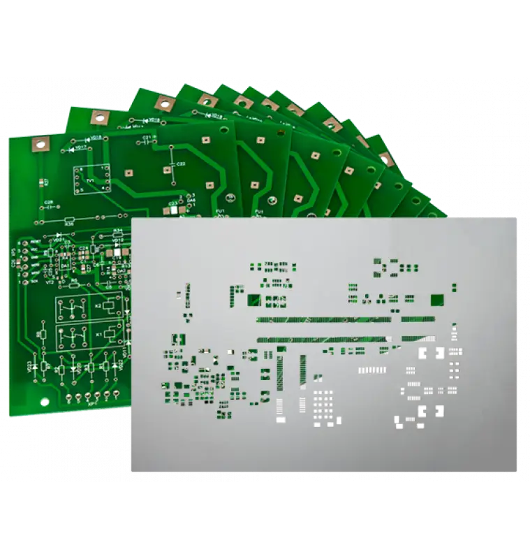
PCB assembly is not a simple process, especially in the printing stage, any small mistakes will cause damage to PCBs or even cause failure. While errors are usually caused by solder joint mounting on PCB pads, the PCB stencil can reduce the chance of errors during the assembly of components. Because of the use of PCB stencils, all solder joints can be mounted on the board at one time, which not only saves a lot of time but also eliminates errors in solder joints. So it’s really important to get a good understanding of PCB stencils. In this guide, we will explain almost everything you need to know about it including types of stencils, PCB stencil design considerations, and also the process of making stencils.
What Is a PCB Stencil?
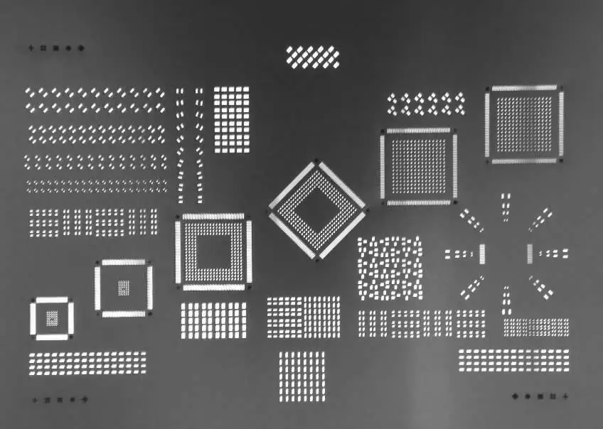
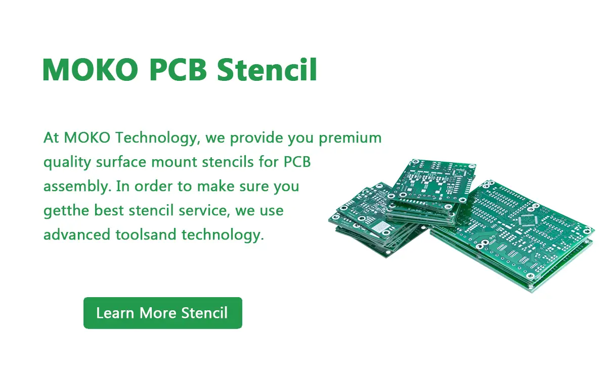
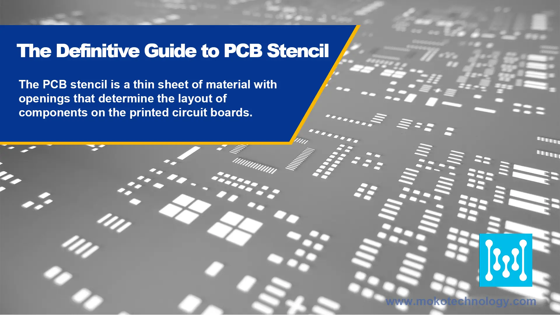
A PCB stencil, also known as a steel mesh, has a primary function of assisting with solder paste deposition. It transfers an exact amount of solder paste to a precise location on the bare printed circuit board. The stencil consists of a stencil frame, wire mesh, and steel sheet. There are numerous openings in the stencil that correspond to the positions requiring printing on the PCB. The solder paste deposits are on the board according to the formation of the stencil holes when the stencil is removed. The PCB stencil helps us to deposit solder paste on designated positions on a bare PCB board so that the electrical connection of the solder joint between the pad and the component can be performed perfectly.
What Is a PCB Stencil Made Of ?
- Frame
Screen frames are mainly categorized into movable and fixed frames. Movable frames directly attach the steel plate to the frame, allowing repeated use of the template frame. Fixed frames adhere the wire mesh to the frame using adhesive. A sturdy frame is achieved through consistent steel tension, typically between 35 and 48 N/cm2.
- Sheet
Materials like copper, stainless steel, nickel alloy, and polyester can be used. Stencils typically utilize premium 301/304 grade stainless steel sheets which have outstanding mechanical characteristics, substantially prolonging the useful life of the stencils.
- Mesh
The mesh fixes the steel plates and frames. Stainless steel or polymer polyester meshes are used. Around 100 mesh stainless steel wire provides sufficient stable tension but can deform and lose tension over time. Polyester mesh is more durable with a longer service life.
- Adhesive
The adhesive binds the mesh frame and steel sheet. It plays a vital role in the template, maintaining strong adhesion and withstanding heavy cleaning with various plate cleaners.
Types of Circuit Board Stencil
The Framed PCB Stencil
It is a laser-cut solder paste stencil that is permanently mounted on the stencil frame, using a mesh border to tightly stretches the stencil foil within a frame. The framed PCB stencil is suitable for high volume screen printing, which can be applied to 16 Mil pitch or below. Framed stencil is featured with smooth aperture walls, good printing performance, and clean laser-cut openings that can also withstand extreme wear.
Frameless Stencil
Frameless PCB stencils, also known as foils, are laser-cut stencils that do not need to be permanently glued into the frame, used with reusable stencil frames called stencil tensioning systems. Frameless SMT stencils offer advanced quality and superior performance at a lower cost than framed stencils. It is suitable for prototype printed circuit board assembly or low-volume production runs, which helps to reduce storage space requirements as well.
Prototype PCB Stencil
Prototype stencils are customized from CAD or Gerber files, when making a prototype PCB template, the template must match the designed PCB prototype. It reduces the possibility of errors when hand soldering prototype PCBs and avoids tedious manual processes. Hence, using such stencils can improve the quality of boards and shorten the assembly cycle of printed circuit board prototypes significantly.
Electroformed Stencil
The electroformed stencil is a nickel-based stencil that is permanently mounted on the stencil frame via a mesh border. The electroformed stencil provides the top solder paste release properties available, so it is ideal for fine pitch SMT applications from 12 mils to 20 mils, as well as flip chip, wafer bumping, and µBGA. Electroformed stencils have a lower coefficient of friction compared to other stencils as they are made of nickel, in addition, they provide extended stencil shelf life.
The Advantages of PCB Stencil
As the circuit boards become more and more complex, the traditional PCB assembly process that requires the manual placing of electronic components before soldering cannot meet the requirements of placing and soldering a large number of small components on smaller circuit boards. We need to use circuit board stencils for machine-operated component placement and solder paste application, which brings a lot of benefits as listed below:
First, PCB stencils help us to improve the accuracy when placing the components on the board, guarantee the fine pitch precision when printing and consequently reduce the possibility of errors.
Second, by using SMT stencils, manufacturers can save more costs and shorten the turnaround time, because circuit board stencils require less labor and time to finish the PCB assembly process.
Third, the stencil facilitates uniform solder application to all surface mount device pads and ensures high pad placement accuracy.
How to Make a PCB Stencil?
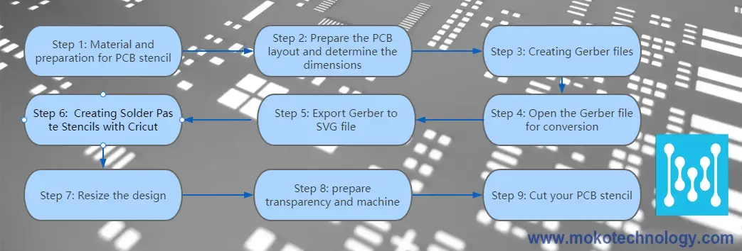
In this part, we will explain the process to create a PCB stencil step by step, there are 9 steps involved:
Step 1: Material and preparation for PCB stencil
Materials
– Cricut machine
– Sure-Cuts-A-Lot software
– Gerber viewer software
– Transparencies for overhead projectors that you can buy at any office supply store
– A Windows XP / Vista computer
Preparation
Your Cricut must have a specific firmware version. You can update/downgrade the firmware by downloading Cricut Design Studio and following the instructions under Help to update the firmware. See the Sure-Cuts-A-Lot FAQ for more information.
Step 2: Prepare the PCB layout and determine the dimensions
It can take some trial and error to create decent solder paste PCB stencils are not very precise. It cuts rounded edges and ignores shapes smaller than about 18mils (0.46mm) by 50mils (1.27mm). That said, you should make sure that all of your component pads are large than these. To make sure a pad still has enough solder paste area, make the pad more. The KiCAD EDA Suite PCB layout program has the ability to change all one footprint pad at a time. Solder has this amazing property that connects to metal parts when reflow finds. As long as your PCB has precise solder resist, solder metal pieces will be found to link. So don’t be too concerned about pads (basically say +/- 20%).
You need the exact dimensions of your PCB template for later. Use your PCB layout software distance tool to determine the distance between the outermost component pads. Not the size of the PCB, but the distance between the outermost pad edges. In the example below, the PCB has a width of 2.3, “but the edge to edge pad distance is 2.142”.
You can measure distances by selecting drawings from the layer pull-down menu and clicking the Dimensions button in the right tool menu. It’s the fourth button from the bottom.
Step 3: Creating Gerber files
Draw your PCB layout using the Gerber solder paste stencil.
When using KiCAD, choose Draw from the File menu. In the plot window, select SoldP_Cmp for the solder paste component layer and click the Plot button.
Step 4: Open the Gerber file for conversion
Open the file in Gerber Gerber Viewer. Select Open Layer (s) from the File menu.
Step 5: Export Gerber to SVG file
Then export the file in SVG format. Select Export, then SVG … from the File menu.
Step 6: Creating Stencils with Cricut
Import the SVG file into Sure-Cuts-A-Lot by choosing Import SVG … from the File menu.
Step 7: Resize the design
Click Keep Proportions in the Properties window and set the stencil’s width to the value previously noted.
Step 8: prepare transparency and machine
Take a sheet of transparency film and cut it to the size of the Cricut cutting mat. Tack the cut transparency into the cutting mat. Place the cutting mat in the machine and press the insert paper button.Set the Cricut’s thrust washer up, the speed wheel will turn to High or Medium, and the cutting blade depth to 5 or 6. Detailed instructions can be found in the Cricut manual. You will find some trial-and-error needed. Speed and pressure can change the accuracy of the cuts, and greater cutting knife depth speeds up how quickly you need to replace the cutting mat.
Step 9: Cut your PCB stencil
Go to cut the design. Choose Cut Design from the Cutter menu.
PCB Stencil Design Considerations
- Thicknessof Stencils
In PCB stencil design, the thickness of stencils is a key factor that would decide the amount of solder paste to be deposited on the board, extra solder deposition would cause solder bridging, while less solder deposition makes the solder joints weak. Normally, the thickness of stencils is from 4 thou to 8 thou.
- Aperture Size
The size of stencil openings needs to be designed smaller than PCB pad size that can avoid problems such as bridging and solder beads, or the solder paste may stick to the aperture walls when the stencils are removed. Therefore, the inner area of the aperture wall should be designed to be two-thirds smaller than the area of the PCB pad to avoid such problems.
- Stencil Material
The material used to make stencils is another factor to consider during PCB stencil design, which affects the ability to release the solder paste from the opening to the PCB pad. The most used material is stainless steel, while for some PCB designs with fine pitch devices, we need to use other materials such as nickel which is 50% more expensive than stainless steel.
- Stencil Alignment
Good alignment of the stencil is critical to get an accurate solder paste print, while to achieve the perfect printing effect, we need to add the fiducial marks to both the PCB and stencil. These fiducials make sure the alignment of the stencil and the printed circuit board is proper.
Ultimately, producing PCB stencils necessitates advanced skills and expertise. If you lack proficiency, collaborating with a trusted PCB stencil manufacturer is recommended. MOKO Technology specializes in PCBA services, providing PCB fabrication, SMT stencil creation, PCB assembly, testing, and shipping services. We have extensive experience in PCBA contract manufacturing. Reach out to a reputable PCB stencil manufacturer like MOKO to get your PCB project underway!