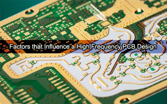
Why are RF PCBs hard to design?

I am a project procurement. Recently, Our project is to develop a television. Of all the materials supply, PCB was the slowest one. And even our engineer took part in the discussion with PCB supplier to push them. Is it really hard to make a RF PCB?

Because radio frequency makes electrons behave differently than they do at lower frequencies or at DC.

At lower frequencies, resistive effects dominate. However, at higher frequencies, impedance and capacitance start to dominate. Also, at higher frequencies, electrons begin to be forced to the surface of a conductor, instead of traveling into the body of the conductor. And the “matching surface” of the dielectric insulator being used to support the conductor also has an effect on electron flow.
The electron exhibits both electronic and magnetic properties as it moves in a conductor. Then magnetic forces can also induce current and noise in nearby adjacent conductors. It causes noise, cross-talk, and eddy currents that disrupt desired operation of a complex circuit.

These effects become more expressed at higher frequencies used. To alleviate this, miniature transmission lines are designed into PCBs with specific physical size and spacing characteristics to make sure these high-speed signals are contained in the transmission lines, and also that the source impedance matches the load impedance as closely as possible.

All of these characteristics require the skilled application of mathematics, board design, and mounted components. It includes accommodations for voltages, currents, resistance, time constants, impedance, impedance matching, logic, and creativity, as well as an innate understanding of the interaction between these interrelated factors.

Read More: High-Frequency PCB

#Consumer Electronic #PCB Design
Oliver Smith

Oliver Smith

Oliver is an experienced electronics engineer skilled in PCB design, analog circuits, embedded systems, and prototyping. His deep knowledge spans schematic capture, firmware coding, simulation, layout, testing, and troubleshooting. Oliver excels at taking projects from concept to mass production using his electrical design talents and mechanical aptitude.
Oliver Smith

Oliver Smith

Oliver is an experienced electronics engineer skilled in PCB design, analog circuits, embedded systems, and prototyping. His deep knowledge spans schematic capture, firmware coding, simulation, layout, testing, and troubleshooting. Oliver excels at taking projects from concept to mass production using his electrical design talents and mechanical aptitude.

What Others Are Asking

How should I handle wet PCBs?

A batch of PCB got wet in warehouse due to roof linking. Too terrible to shoulder the lost. How can I do to rescue these wet PCBs? Or to minimize the damage?

Where is the ground located in a PCB?

I am learning to design a multiple layer board for a medical device, and have a question about where the ground should place.

Read Detailed Advice From Blog Articles

PCB Stackup Design Guide
Ryan Chan

PCB Stackup Design Guidelines

People expect electronic products to be rich in functions, but also require them to be small and portable, which brings new challenges to circuit board

microwave pcb
Ryan Chan

16 Steps On Microwave PCB Design

Printed circuit boards with high-speed chips and microwave PCB structures have numerous parameters that differ significantly from those of conventional, rigid and flexible printed circuit

Scroll to Top
Scroll to Top