Can I leave a through hole pad off one side of a machine-fabricated PCB?

I'm designing a two-layer PCB and I'm very inexperienced. A third-party company will fabricate them. Now, I have a PTH part with a number of closely spaced pins. However, I can't greatly simplify routing by running traces unless I eliminate the pads for certain pins on one side of the board. So can I leave a through hole pad off one side of a machine-fabricated PCB?

It will be flagged as a defect if inspected by IPC-610 (Class 1,2 or 3). So what you’re trying to do is not acceptable. Damage to one of the pads (top or bottom) is also a defect.

I have seen boards where the pad is not a perfect circle (like an ellipse) to make space for traces to go in between. This seems acceptable.

Read More: Through Hole PCB Assembly

#PCB Design #PCB Assembly
Picture of Oliver Smith

Oliver Smith

Oliver is an experienced electronics engineer skilled in PCB design, analog circuits, embedded systems, and prototyping. His deep knowledge spans schematic capture, firmware coding, simulation, layout, testing, and troubleshooting. Oliver excels at taking projects from concept to mass production using his electrical design talents and mechanical aptitude.

What Others Are Asking

CEM3 or FR4 PCB, which is the lightest material?

There is nothing about weight in the substrate datasheets I found.
Between CEM-3 or FR4, which is the lightest material ? What is the average weight by surface for CEM-3 boards ?

Why does flexible PCB need stiffeners?

When I browsed some comments online, I see someone recommends stiffeners to apply on flexible PCB. Very confused about that? Is it a formal design?

How is the panel separated after assembly?

I need to design LED tube PCB and is only 20mm wide, so there will be at least 10 pieces next to each other on one panel. The assembly house warned me, that it is not the same to separate these as it is with standard PCBs. How are these made to be separated?

Read Detailed Advice From Blog Articles

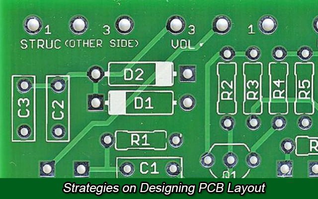
Strategies on Designing PCB Layout
Ryan Chan

Strategies on Designing PCB Layout

Why PCB Layout is Needed We use Printed Circuit Boards (PCB) for connecting electronic components by using conductive tracks. This allows for prototyping electric circuits

Flex PCB Design
Ryan Chan

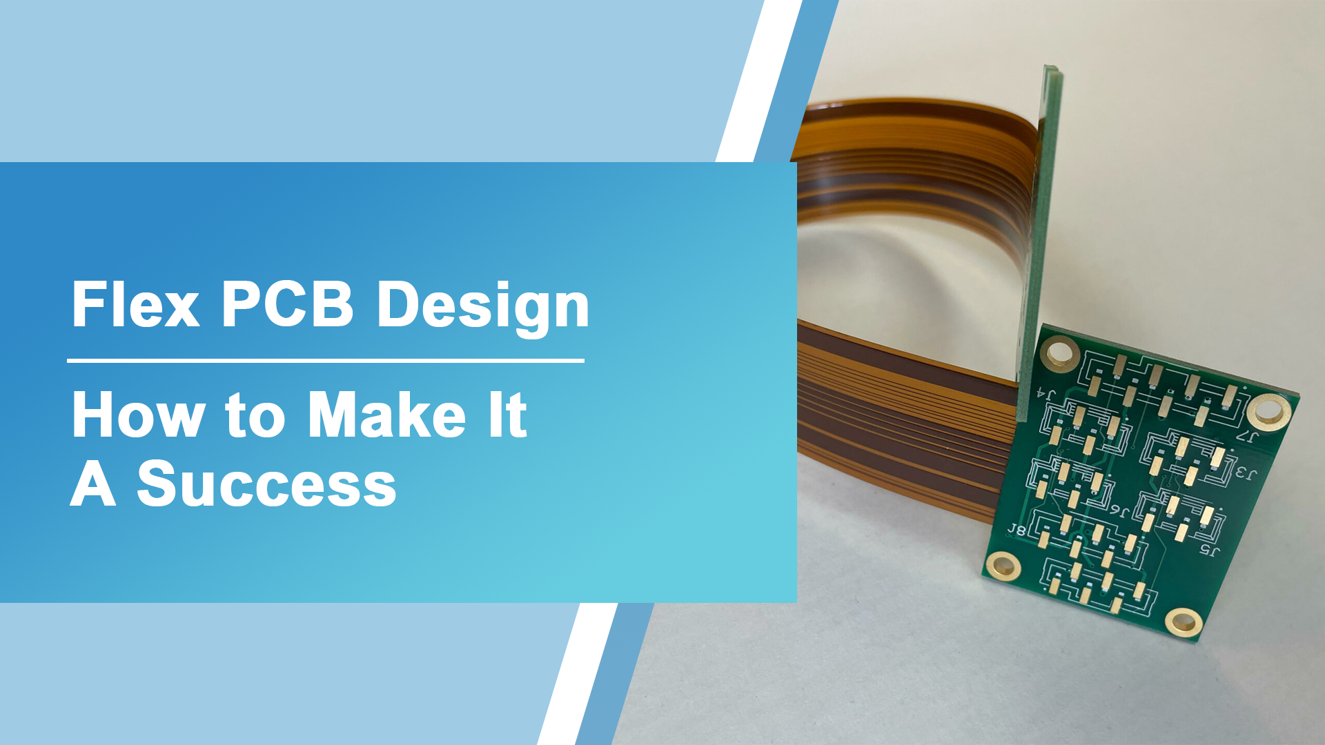
Flex PCB Design- How to Make It A Success

Flex PCBs, or Flexible Printed Circuit Boards, have gained significant popularity in recent years due to their unique properties and advantages in various applications. These

Scroll to Top