How much larger should a plated-through hole be than lead diameter to get good solder wetting?

I'm designing a new PCB where I have a whack of connectors that have to line up with the metalwork. There are some problematic connectors. All 4 pins are round. I want to have the holes as small as possible while allowing for good solder adhesion over the full length of the pin. I'm looking for guidance on how much clearance around the component lead I should have in order to get good solder wetting and adhesion.

I don’t think you should depend on the holes to locate the part when tolerances are important. I think 10-15 mils is good solution(in metric 0.25 to 0.4mm).

Make up a jig to hold the parts in the proper location while they are being soldered. It can be fancy for wave soldering or something simple that holds the parts while being hand soldered (perhaps fashioned from the mating part such as the punched chassis).

Round pins are a particular hassle if you call it too close- at least with square or rectangular pins you can skive off some plating inside the holes at the corners of the pin and still force the pin in. If you insist on the using the holes, maybe make the peg round and the hole square (call out slot-drilled square holes in the PCB).

Read More: THT PCB Assembly

#PCB Assembly

Picture of Oliver Smith

Oliver Smith

Oliver is an experienced electronics engineer skilled in PCB design, analog circuits, embedded systems, and prototyping. His deep knowledge spans schematic capture, firmware coding, simulation, layout, testing, and troubleshooting. Oliver excels at taking projects from concept to mass production using his electrical design talents and mechanical aptitude.

What Others Are Asking

How does a PCB Prototype look like?

It is the first time I place a prototype order to a manufacturer for my research. And I want to know how a common prototype looks like.

Read Detailed Advice From Blog Articles

what are PCB pads?
Will Li

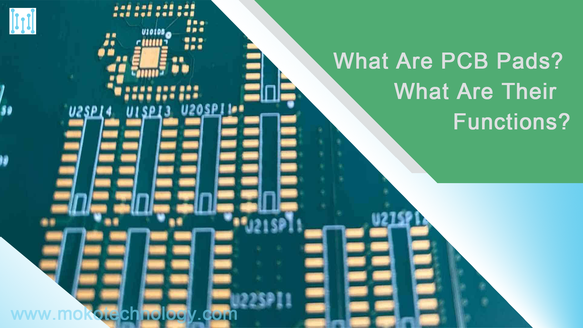
What Are PCB Pads? What Are Their Functions?

In the manufacturing process of PCBA, soldering is a very important process, which is used to achieve the electrical connection between all components and the printed

Scroll to Top