Thick copper PCB has no fixed IPC definition. Usually, we define a robust printed circuit board as using three or more ounces of copper in the inner and/or outer layers of a printed circuit board or a power distribution board. Some companies are UL certified for up to 6 ounces of copper on the interior and exterior layers, and they are capable of producing coated, non-plated printed circuit boards using up to 20 ounces of copper for both sides and multiple layers.
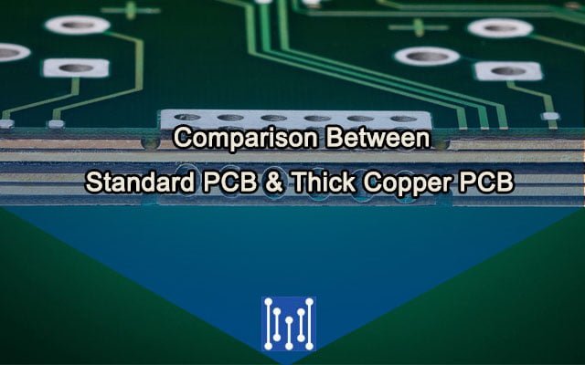
Comparison between Standard PCB & Thick Copper PCB
Thick PCB products are widely used in power electronics and power systems. A trend towards increased production of printed circuit boards, this unique type of copper printed circuit board has a final copper weight of more than 4 ounces (140μm), compared with 1-ounce copper (35μm) or 2 ounces (0μm) in total those with standard copper plate thickness.
The extra thickness of copper printed circuit boards allows the plate to conduct a higher current, obtain a proper heat distribution, and perform complex switches in a limited space. Other advantages include increased mechanical strength in sections of conductors, the ability to create smaller products by incorporating several weights in the same layer of the circuit, and the ability to use exotic materials with maximum capacity with minimal risk of circuit failure.
The Thick Copper PCB Fabrication
Mil/Aero high-power electronic products place new demands on printed circuits, creating thick copper printed circuits or even extreme copper printed circuits. Thick copper printed circuit boards refer to printed circuit boards in which the thickness of the copper conductor varies from 137.2 to 686 microns, while printed circuit boards with a thickness of copper exceeding 686 microns or up ‘at 6860μm are printed circuit boards with extreme copper.
The advantages of designing thick copper circuit boards include:
- Capable of withstanding thermal stresses while improving the anti-stress capacity of the printed circuit board
- Increases the capacity of the printed circuit board
- Increased heat dissipation of the printed circuit board without the need to collect cooling fins
- It increases the mechanical resistance of the joint between the layers and the through-holes
- It applies to high power flat panel transformers placed on board
Everything has two sides. In addition to these advantages, heavy copper printed circuit boards have many disadvantages. It is essential to know both sides of heavy copper circuit board designs to be able to understand how to use potential functions and applications.
Thick Copper PCB Capabilities
There are a lot of purposes that are fulfilled by the heavy copper PCB and maybe some things that we use nowadays couldn’t be achieved without it. But what capabilities make it different from the other PCBs? We’ll be discussing these things below:
Numerous designs need particular copper thicknesses to fulfill the current needs of a specific design. PCB manufacturers provide a different range of copper weights to allow you to meet all of the requirements of your project.
Copper Weight
Copper weight is the weight in ounces of the copper used in a sq. foot of area. This shows the thickness of copper on the layer as a whole. Most of the companies use different copper weights for Printed Circuit Board manufacturing. The suitable copper weight can be selected to fulfill the requirements of a design.
Inner Layers
The inner layers are similarly recognized as the internal layers of a heavy copper printed circuit board.
The thickness of the sheet and dielectric, as well as the copper mass of the inner layers, is predetermined for the standard projects.
By choosing a custom design according to the order and loading the desired package of materials, you can adjust the thickness and weight of copper in these internal layers to suit your needs. Minimum product widths and distances are based on the weight of the copper layer.
The inner layers sometimes use the technique of “copper pour.” Engraving is commonly used to create a strong ground plane or power plane. Another benefit of using copper casting is to reduce the amount of chemical compound (ethanol) used in the manufacturing process (better for the environment), and also helps the process of bonding layers with layers.
The inner layers can be transferred for fabrication with positive or negative polarity. It is important that the polarity of the layer be noted during the successive process in the absence of a particular polarization characterization (i.e., thermal relationship).
Outer Layers
The outer layers are also recognized as the external copper layers of the printed circuit board. Typically, electronic components are bonded to the outer layers by soldering them through holes or on the surface.
The outer layers usually start with copper foil, which is then galvanized with copper to increase the thickness and add copper to the through-hole drums. The copper weight of the outer layers is predefined for standard designs. However, the finished copper thickness of these layers can be customized to meet your needs by selecting a custom assembly during the sorting process and loading the repository into your file. The widths and the minimum achievable distances are based on a pre-plate (sheet) mass of the layer.
The capabilities mentioned above make the thick copper PCB a good choice to be used in the products. There are many companies that offer the services to make the thick copper PCBs and the capabilities may differ from manufacturer to manufacturer. You should not compromise on the quality of the PCB because it defines the overall performance of the product. Using a good PCB may look like a lot of burden on your finances, but in reality, it is the opposite. Yes, the PCBs reduce the cost and increase the quality of an electronic device.
MOKO Technology offers the best solutions for all your PCB needs with the right pricing. The offer the PCBs with the right weight and that can fulfill all of your PCB needs for a range of products.