What are the black spots in lead-free solder joints on PCB?

I am prototyping a PCB, using Chip Quik's "SMDSWLF.031, a Sn96.5/ Ag3.0/ Cu0.5 solder with 2.2% no-clean flux. I find that the black spots appears frequently in larger pads on my board. I wonder if it is because I left the soldering iron more time heating the solder and that burnt the flux. What is that black residue? Is that a sign of a bad joint or maybe bad soldering technique?

Those dark splotches may be leftovers from the resin-based flux. No-clean fluxes are often made out of water-soluble resins (vs rosin) and during heating, most of it will evaporate away.

Pay attention to soldering temperatures. Sn96.5/Ag3.0/Cu0.5 solder’s liquidus is 217 °C. Soldering at high temperatures you have been using can potentially damage components, has been weakening the glue under every pad you solder (the copper is glued to the FR4), producing significantly more hazardous fumes, something that is already more hazardous with lead-free solders, and generally does nothing good.

As far as I know, it should not have a meaningful impact on the joint, but if you want to avoid this, I suggest lowering your iron temperature (and possibly getting a new tip and/or iron depending, so soldering is effective at said lower temperature), though this may not totally resolve the issue.

Read More: PCB Prototype

#PCB Assembly #PCB Design
Picture of Oliver Smith

Oliver Smith

Oliver is an experienced electronics engineer skilled in PCB design, analog circuits, embedded systems, and prototyping. His deep knowledge spans schematic capture, firmware coding, simulation, layout, testing, and troubleshooting. Oliver excels at taking projects from concept to mass production using his electrical design talents and mechanical aptitude.

What Others Are Asking

How can I fix the PCB to the mechanical structure?

I designed a PCB with an imaging sensor that is mechanically coupled to a lens assembly using four 2-56 screws. I’m noticing that even though the screws are holding the board tightly against the mechanical structure if I flick or lightly knock the the assembly the image “moves”.  I’m hoping to get a few suggestions for ways to fix the PCB to the mechanical structure. Any suggestions for adhesives or the like? Something else?

How do you handle a PCB that didn’t print correctly?

I did have one board come back with a manufacturer error – an extra bit of copper just a hair’s width across hidden underneath a component. It looked almost like someone’s eyelash had fallen onto the board just before photo etch. How should I deal with it?

Read Detailed Advice From Blog Articles

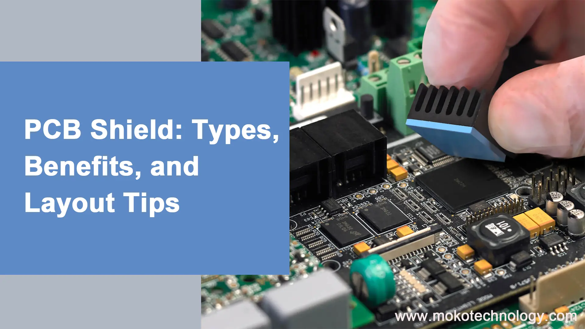
PCB Shield: Types, Benefits, and Layout Tips
Ryan Chan

PCB Shield: Types, Benefits, and Layout Tips

Printed circuit board (PCB) designers often grapple with electromagnetic interference when laying out boards. They must consider electromagnetic compatibility to satisfy system specs. Even small

Scroll to Top