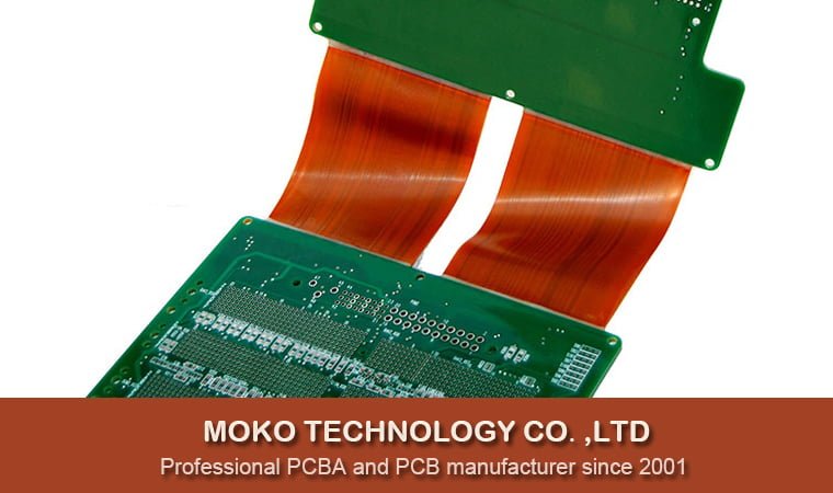
Are you thinking about incorporating a flex circuit into your product? These boards are perfect choices for various applications due to their incredible characteristics. With the demand for flexible PCBs projected to surge in the future, their presence in electronic devices will become ubiquitous. This article will guide you about the different important aspects. For example, what is the process of flexible PCB manufacturing, and which factors you should consider before purchasing and manufacturing circuit boards?
Flexible PCB Manufacturing Process
Step 1: Flex circuit design
The first step in flex PCB manufacturing is to use CAD ( computer-aided design) software to design the flexible printed circuit board, including the layout of the circuit, placement of components, and so on.
Step 2: Material selection
The most common materials for manufacturing flexible PCBs are polyimide (PI) and polyester (PET) films because they have excellent electrical insulation properties and flexibility, and are also very resistant to high temperatures. The specific choice of material depends on the application environment, solder mask requirements, electrical requirements, etc.
Step 3: Circuit pattern exposure
Circuit pattern exposure is a key step in the flexible PCB manufacturing process. In this process, the circuit pattern design is transferred to the copper-clad laminate material of the circuit board.
Step 4: Etching
Next, we need to do PCB etching. It is a process to remove unnecessary copper material from the PCB by using an etchant solution. As a result, the circuit pattern as designed is formed. During this step, the drilled hole locations are also exposed to facilitate subsequent hole formation.
Step 5: Stiffener Application
In some cases, stiffeners are needed to provide structural reinforcement. They are typically rigid materials such as FR-4 (epoxy-glass composite) or polyimide. Applying stiffeners to specific areas on the board can also prevent excessive bending in these areas.
Step 6: Drilling and plating
Carefully drill holes at the designated spots on the PCB to create through-holes. These holes enable you to later insert and solder components directly onto the board. Following the drilling process, the holes are plated to ensure conductivity between layers.
Step 7: Applying Coverlay
At this stage, durable polyimide coverlay panels are carefully aligned and affixed onto the production panels before the lamination process. The coverlays can protect components from potential damage during subsequent manufacturing steps.
Step 8: Component Assembly
Once the Flex PCB is fabricated, components need to be mounted onto the board. Commonly used assembly techniques are surface mount technology (SMT) and through-hole mounting.
Further reading: Through Hole Vs. Surface Mount: How to Choose the Right Method
Step 9: Testing and inspection
Lastly, each PCB undergoes electrical testing to identify any shorts, opens, and to verify that the impedance aligns with the design specifications. In addition to this, both visual and automated inspections are carried out meticulously to detect any physical defects or assembly anomalies.
What to Consider before Flexible PCB Manufacturing?
The usage of flex circuits offers you a huge variety of interconnections and reliability. Moreover, they offer lighter weight, durability and compressed construction. There are different materials and manufacturing options are available for flex boards. This new emerging technology has a bright future. So here are some important things you need to consider before manufacturing it:
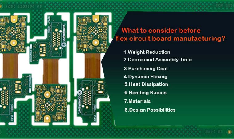
Weight Reduction
By utilizing flexible circuits, you can reduce the weight of different electronic packages. It is because they don’t have reinforcements. In addition, they are higher in density as compared to unfilled polymers. So you should choose a suitable material for weight reduction.
Decreased Assembly Time
If the circuit boards are more flexible, it means they won’t break during manufacturing. Flex circuit boards are not fragile so there is the least risk of breakage.
Purchasing Cost
Most people consider it costly. Yes, it is a fact that flexible circuits are costly. However, if you have a look at the price and durability, it may outrun the cost. All you need to pick a reliable manufacturer. Reliable manufacturers provide durable and long-lasting circuit boards. Thus, if you spend a few extra bucks, it will not get wasted.
Dynamic Flexing
It is another important factor to buy polyimide having extremely thin copper foil. It is ideal for different dynamic flexing applications. You can use a thicker flex for a bend and stay application.
Heat Dissipation
Heat dissipation is better on the flat copper tracks. Instead of wire surrounded by insulation material. It makes the flexible circuit the finest choice in different applications. The application in which heat resistance is a crucial factor.
Flexible circuits are more resistant to heat as compared to other types of PCBs. So always consider this factor for circuit boards to resist heat. Luckily, the flex circuit has this capability by default.
Bending Radius
It depends on the thickness of copper and the overall thickness of the circuit boards. Moreover, it also depends on the number of total bending layers. Here are the flex circuit types and their least bending capabilities:
A single-sided flex circuit contains 3 to 6 times bending capability. Double-sided flex circuits offer 7 to 10 times bending capability. Dynamic flex application contains almost 20 to 40 times bending ability.
Materials
Polyimide is the most common material for flex circuits. Some other materials are also available for board construction such as LCP(liquid crystal polymers) and PEN(Polyethylene naphthalate). If you want reliable products, polyimide is the top priority.
Advantages of Polyimide
Here are a few pros of polyimide:
- Ideal flexibility at all temperatures
- Having excellent electrical priorities
- Containing amazing resistance ability against tear and chemicals.
- The highest tensile strength
Disadvantages of Polyimide
Here are a few cons of polyimide:
- It is quite expensive than PEN.
- If you use it with an adhesive system, temperature performance becomes worse.
- Polyimide absorbs moisture up to 3%.
Design Possibilities
Flex circuit boards have a lot of design possibilities. You can customize the design of FPCB according to your needs and requirements.
Challenges of Flex PCB Manufacturing and Solutions
Designing and manufacturing flex PCB comes with some challenges. Below we list the most prevalent issues encountered with flex circuits, along with their solutions:
Solder mask
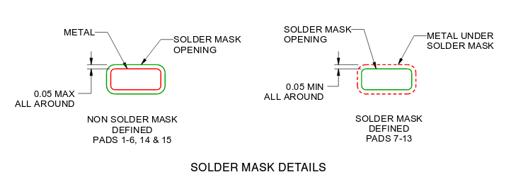
While applying the cover film or solder mask, it can affect underlying traces. The PCB manufacturers should take these factors into account while manufacturing FPCB. The design and construction procedure should compensate for these shortcomings.
Solder Pads
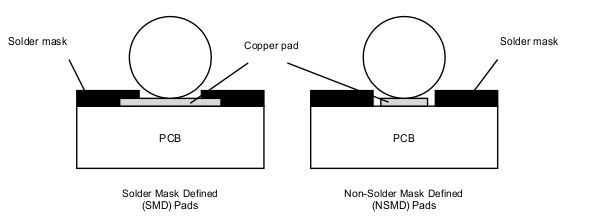
There must be enough space between the copper trace and solder pad. If manufacturers fail to implement this condition, it can affect reliability. Moreover, it also affects the durability of the flexible PCB. The solution to this problem is straightforward. Employing a team of expert engineers to oversee the manufacturing process can prevent these issues.
Solder Joints
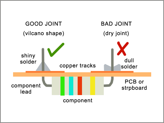
It is a procedure to join copper trace and solder alloy by using solder. Solder mask can cover an entire space of the circuit boards. Sometimes trace becomes very rigid if an inexperienced member of this. Poor solder joints can easily lead flexible PCBs to crack during folding or bending. Thus, it is important to do this job by a proficient engineer for durability and reliability.
Choose MOKO Technology as Your Flex PCB Manufacturer
MOKO Technology is China’s top flexible PCB manufacturer with nearly 20 years of PCB manufacturing experience. Utilizing our professional knowledge and manufacturing capabilities in circuits, we provide clients with customized solutions for flex PCB fabrication. From design to assembly and testing, we provide a one-stop PCB service. Contact us to get a free quote now.